Spi registers, Spi register description – Ocean Optics EMBED2000+ User Manual
Page 8
EMBED2000+ Data Sheet
8
029-20000-005-05-201305
SPI Registers
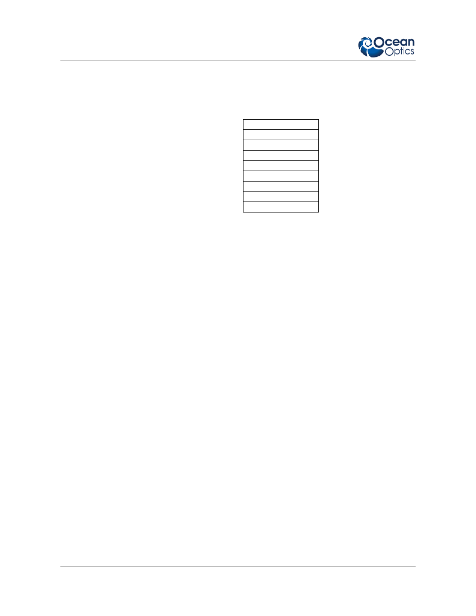
Below is a table containing the available register addresses for FPGA configuration and operation.
Address
FPGA_VERSION
0x04
Read Only
FPGA_COUNTBASE
0x08
Read/Write
FPGA_STRBCOUNT
0x0C
Read/Write
FPGA_INTCLOCK
0x18
Read/Write
FPGA_SSLOWDELAY
0x38
Read/Write
FPGA_SSHIGHDELAY
0x3C
Read/Write
FPGA_LAMPENABLE
0x40
Read/Write
FPGA_OFFSETVALUE
0x5C
Read/Write
FPGA_MAXSATVALUE
0x68
Read/Write
SPI Register Description
FPGA_VERSION
- 0x04
A read from this register provides the current FPGA configuration version.
FPGA_COUNTBASE - 0x08
This register divides provides a base frequency counter for the Continuous strobe function.
CS_BasePeriod = FPGA_COUNTBASE / 48MHz
FPGA_STRBCOUNT
- 0x0C
This register uses the COUNTBASE register at address 0x08 to form the Continuous Strobe
signal.
ContStrobe = (FPGA_STRBCOUNT + 1) * CS_BasePeriod
FPGA_INTCLOCK
- 0x18
This register is used to generate the detector integration time represented in milliseconds.
Values of 1 to 0xFFFF are used for integration times of 1ms and 65.535s.
FPGA_SSLOWDELAY -0x38
This value corresponds to the time delay that the SingleStrobe signal goes low after the start
of an integration time.
FPGA_SSHIGHDELAY -0x3C
This value corresponds to the time delay that the SingleStrobe signal goes high after the start
of an integration time.
Note:
The value in LOWDELAY must be higher than HIGHDELAY in order for a strobe to be
present.
FPGA_LAMPENABLE -0x40
The least significant bit of this register is the global enable (1) and disable (0) for both the
Continuous Strobe and Single Strobe functions present on Hirose Pin 14 and 15, respectively.