Fpga communication, Spi communication examples – Ocean Optics EMBED2000+ User Manual
Page 7
EMBED2000+ Data Sheet
029-20000-005-05-201305
7
FPGA Communication
The SPI bus is the I/O communication link between the controlling device and FPGA. The FPGA is
considered the slave device and handles up to an 8MHz SPI clock for decoding MOSI bitstreams.
Data on MOSI is clocked in on the falling edge of the SPI clock, while data out to MISO is latched on
the rising edge.
SPI Communication Examples
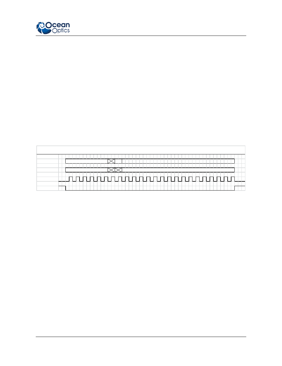
Each read and write transfer is 24 clock pulses total consisting of 6 address bits, a null bit, a R/W bit
0/1 respectively, and 16 data bits.
The MOSI bitstream is decoded on the rising edge of each SPI_CLK. All values returned from a read
cycle transition on the falling edge of SPI_CLK.
Below is an example of a single generic SPI read/write cycle.
MOSI
MISO
SPI_CLK
SPI_CS
Address
R/W
SPI Generic Read / Write Cycle
16-bit Read Data
Address
- Apex 785 Raman (1 page)
- STS-UV (2 pages)
- TR2 Engineering Note (4 pages)
- SAD500 Communications and Control (19 pages)
- Red Tide USB650 Install (26 pages)
- Fiber Optic Termination Kit (6 pages)
- Transmissive pH Probe (10 pages)
- Remora (42 pages)
- PlasCalc (59 pages)
- Correcting Device Driver Issues (8 pages)
- ecoVis Krypton Light Source (16 pages)
- LPC-500CM (28 pages)
- HPX-2000 (24 pages)
- ADC1000-USB (27 pages)
- Torus Operating Instructions (30 pages)
- ADC2000-PCI (13 pages)
- Sensors for Real-Time Analysis (2 pages)
- IDRaman reader (2 pages)
- DH-2000-CAL (30 pages)
- QE65 Pro (32 pages)
- Collimating Lenses (2 pages)
- D1000 (2 pages)
- IDRaman mini (2 pages)
- HR2000CG-UV-NIR (42 pages)
- Cool Red (1 page)
- HL-2000 (20 pages)
- XE-1 Xenon (6 pages)
- USB-ADP Serial Adapters (3 pages)
- CHEM2000 (36 pages)
- Deuterium-Halogen Calibration Light Source (19 pages)
- NeoFox Engineering Note (30 pages)
- QE Pro (2 pages)
- OOIBase32 (140 pages)
- AR-1 Argon (6 pages)
- pH Sensor Patches, Probes and Cuvettes (36 pages)
- SpecLine Offline Spectroscopy (60 pages)
- HL-2000-HP-232 (26 pages)
- External Triggering Options Instructions for Spectrometers with Firmware Version 3.0 and Above (16 pages)
- Breakout Box (10 pages)
- USB-ISS-UV_VIS (4 pages)
- ISS-UV_VIS (6 pages)
- OOIColor (14 pages)
- LS-1 Series (12 pages)
- Apex Install (24 pages)
- DH-2000 (34 pages)