Rtc address map – Rainbow Electronics DDS1693 User Manual
Page 6
DS1689/DS1693
6 of 32
When 5-volt operation is selected, the device is fully accessible and data can be written and read only
when V
CCI
is greater than 4.5 volts. When V
CCI
is below 4.5 volts, read and writes are inhibited. However,
the timekeeping function continues unaffected by the lower input voltage. As V
CC
falls below the greater
of V
BAT
and V
BAUX
, the RAM and timekeeper are switched over to a lithium battery connected either to
the V
BAT
pin or V
BAUX
pin.
When 3-volt operation is selected and applied within normal limits, the device is fully accessible and data
can be written or read. When V
CCI
falls below V
PF
, access to the device is inhibited. If V
PF
is less than
V
BAT
and V
BAUX
, the power supply is switched from V
CCI
to the backup supply (the greater of V
BAT
and
V
BAUX
) when V
CCI
drops below V
PF
. If V
PF
is greater than V
BAT
and V
BAUX
, the power supply is switched
from V
CCI
to the backup supply when V
CCI
drops below the larger of V
BAT
and V
BAUX
.
When V
CC
falls below V
PF
, the chip is write-protected. With the possible exception of the
KS
,
PWR
, and
SQW pins, all inputs are ignored and all outputs are in a high impedance state.
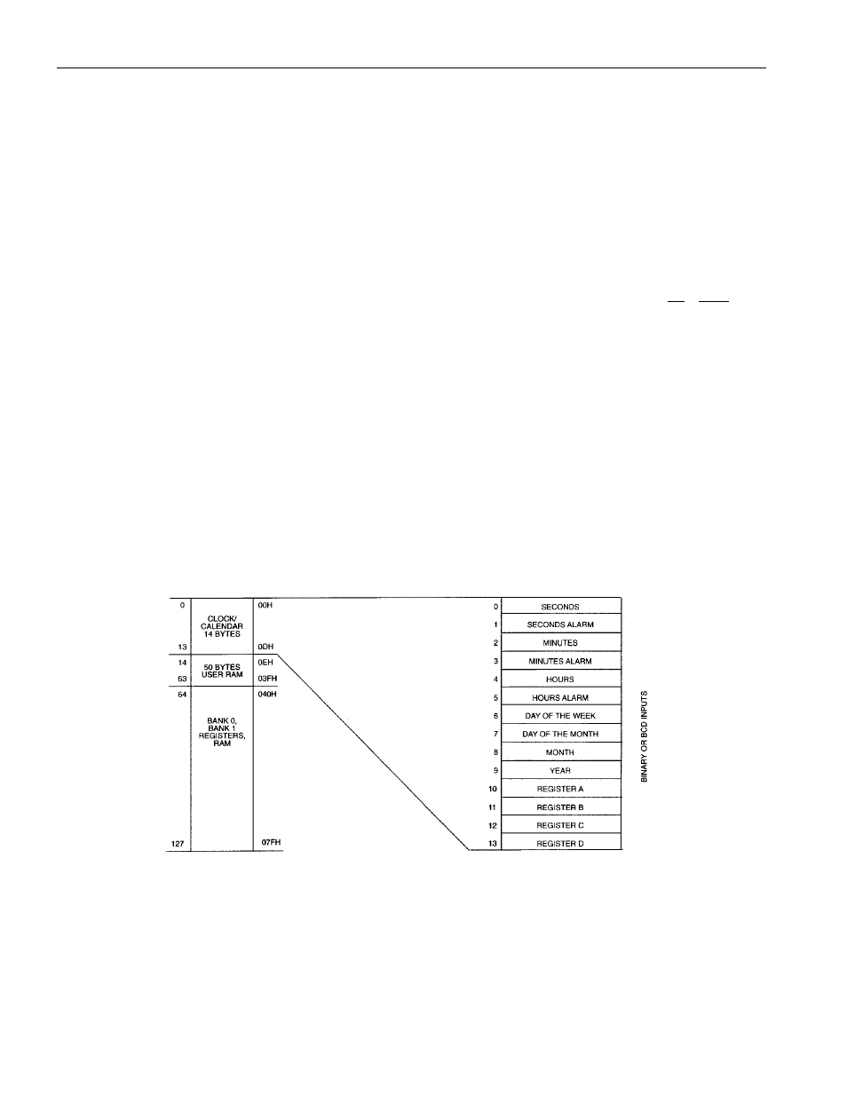
RTC ADDRESS MAP
The address map for the RTC registers of the DS1689/DS1693 is shown in Figure 2. The address map
consists of the 14-clock/calendar registers. Ten registers contain the time, calendar, and alarm data, and
four bytes are used for control and status. All registers can be directly written or read except for the
following:
1. Registers C and D are read-only.
2. Bit 7 of Register A is read-only.
3. The high order bit of the seconds byte is read-only.
DS1689 REAL TIME CLOCK ADDRESS MAP Figure 2