Design procedure – Rainbow Electronics MAX3798 User Manual
Page 27
Design Procedure
Programming Bias Current
1) IBIASMAX[7:0] = Maximum_Bias_Current_Value
2) SET_IBIAS
i
[8:1] = Initial_Bias_Current_Value
Note: The total bias current value is calculated using
the SET_IBIAS[8:0] register. SET_IBIAS[8:1] are the bits
that can be manually written. SET_IBIAS[0] can only be
updated using the BIASINC[7:0] register.
When implementing an APC loop it is recommended to
use the BIASINC[7:0] register, which guarantees the
fastest bias current update.
3) BIASINC
i
[4:0] = New_Increment_Value
4) If (SET_IBIAS
i
[8:1]
≤ IBIASMAX[7:0]),
then (SET_IBIAS
i
[8:0] = SET_IBIAS
i-1
[8:0] + BIASINC
i
[4:0])
5) Else (SET_IBIAS
i
[8:0] = SET_IBIAS
i-1
[8:0])
The total bias current can be calculated as follows:
6) I
BIAS
= [SET_IBIAS
i
[8:0] + 20] x 40μA
Programming Modulation Current
1) IMODMAX[7:0] = Maximum_Modulation_Current_Value
2) SET_IMOD
i
[8:1] = Initial_Modulation_Current_Value
Note: The total modulation current value is calculated
using the SET_IMOD[8:0] register. SET_IMOD[8:1] are
the bits that can be manually written. SET_IMOD[0] can
only be updated using the MODINC[7:0] register.
When implementing modulation compensation, it is rec-
ommended to use the MODINC[7:0] register, which
guarantees the fastest modulation current update.
3) MODINC
i
[4:0] = New_Increment_Value
4) If (SET_IMOD
i
[8:1]
≤ IMODMAX[7:0]),
then (SET_IMOD
i
[8:0] = SET_IMOD
i-1
[8:0] + MODINC
i
[4:0])
5) Else (SET_IMOD
i
[8:0] = SET_IMOD
i-1
[8:0])
The following equation is valid with assumption of 100
Ω
on-chip and 100
Ω external differential load (Rextd). The
maximum value that can be set for SET_TXDE[3:0] = 11.
6)
I
MOD(Rextd=100
Ω)
= [(20 + SET_IMOD
i
[8:0]) x 40μA]
For general Rextd, the modulation current that is
achieved using the same setting of SET_IMOD
i
[8:0] as
for Rextd = 100
Ω is shown below. It can be written as a
function of I
MOD(Rextd=100
Ω)
, still assuming a 100
Ω on-
chip load.
7)
Programming LOS Threshold
LOS
TH
= (SET_LOS[7:0] x 1.5mV
P-P
)
Programming Transmit Output
Deemphasis
The TXDE_EN bit must be set to 1 to enable the deem-
phasis function. The SET_TXDE register value is used
to set the amount of deemphasis, which is a percent-
age of the modulation current. Deemphasis percentage
is determined as:
Where the maximum SET_TXDE[3:0] = 11.
For an I
MOD
value of 10mA, the maximum achievable
deemphasis value is approximately 20%. Maximum
deemphasis achievable for full I
MOD
range of 12mA is
limited to 15%.
With deemphasis enabled, the value of the modulation
current amplitude is reduced by the calculated deem-
phasis percentage. To maintain the modulation current
amplitude constant, the SET_IMOD[8:0] register must
be increased by the deemphasis percentage. If the sys-
tem conditions like temperature, required I
MOD
value,
etc., change during the transmit operation, the deem-
phasis setting might need to be readjusted. For such an
DE
SET TXDE
(%)
_
[ : ]
=
×
+
(
)
100
2
3 0
64
I
I
xt
xt
MOD
xtd
MOD
xtd
(Re
)
(Re
)
Re
Re
= ×
+
⎡
=
Ω
2
100
100
⎣⎣⎢
⎤
⎦⎥
×
− +
⎡
⎣⎢
⎤
⎦⎥
_
[ : ]
1
2
3 0
64
SET TXDE
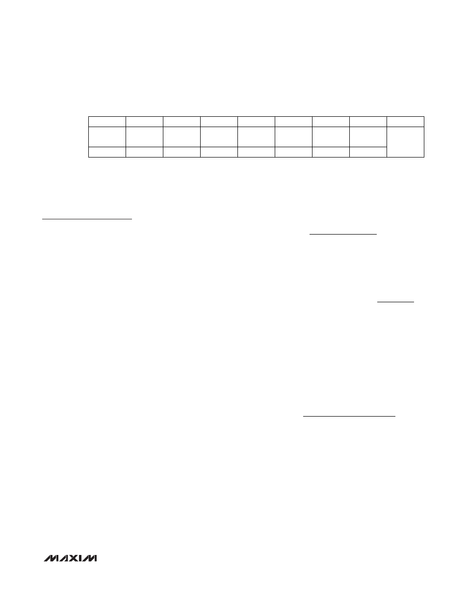
Transmitter Deemphasis Control Register (SET_TXDE)
Bits 3 to 0: SET_TXDE[3:0]. This is a 4-bit register used to control the amount of deemphasis on the transmitter out-
put. When calculating the total modulation current, the amount of deemphasis must be taken into account. The
deemphasis is set as a percentage of modulation current.
MAX3798
1.0625Gbps to 10.32Gbps, Integrated, Low-
Power SFP+ Limiting Amplifier and VCSEL Driver
______________________________________________________________________________________
27
Bit #
7
6 5 4 3 2 1 0
ADDRESS
Name
X X X X
SET_TXDE
[3] (MSB)
SET_TXDE
[2]
SET_TXDE
[1]
SET_TXDE
[0] (LSB)
Default
Value
X X X X 0 0 0 0
H0x10