Max3798, Detail description, Pin description (continued) – Rainbow Electronics MAX3798 User Manual
Page 14
MAX3798
Detail Description
The MAX3798 SFP+ transceiver combines a limiting
amplifier receiver with loss-of-signal detection and a
VCSEL laser driver transmitter with fault protection.
Configuration of the advanced Rx and Tx settings of the
MAX3798 is performed by a controller through the
3-wire interface. The MAX3798 provides multiple cur-
rent and voltage DACs to allow the use of low-cost con-
troller ICs.
Limiting Amplifier Receiver
The limiting amplifier receiver inside the MAX3798 is
designed to operate from 1.0625Gbps to 10.32Gbps.
The receiver includes a dual path limiter, offset correc-
tion circuitry, CML output stage with deemphasis, and
loss-of-signal circuitry. The functions of the receiver can
be controlled through the on-chip 3-wire interface. The
registers that control the receiver functionality are
RXCTRL1, RXCTRL2, RXSTAT, MODECTRL, SET_CML,
and SET_LOS.
1.0625Gbps to 10.32Gbps, Integrated, Low-
Power SFP+ Limiting Amplifier and VCSEL Driver
14
______________________________________________________________________________________
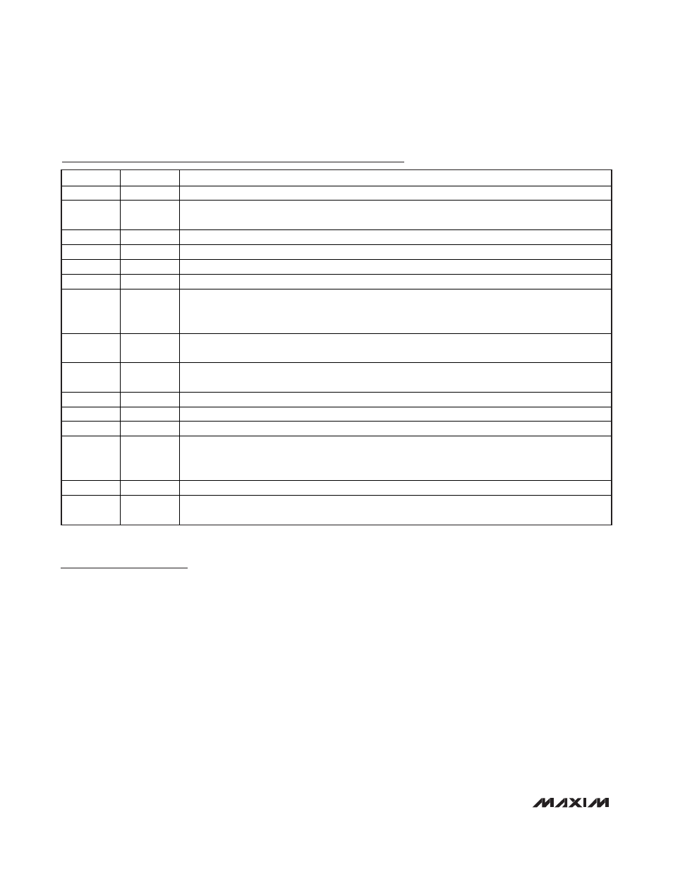
Pin Description (continued)
PIN
NAME
FUNCTION
14
TIN-
Inverted Transmit Data Input, CML
16 BMON
Bias Current Monitor Output. Current out of this pin develops a ground-referenced voltage across an
external resistor that is proportional to the laser bias current.
17 V
EET
Ground. Provides ground for the transmitter block.
19
TOUT-
Inverted Modulation Current Output. Back-termination of 50
to V
CCT
.
20
TOUT+
Noninverted Modulation Current Output. Back-termination of 50
to V
CCT
.
22
BIAS
VCSEL Bias Current Output
23 FAULT
Transmitter Fault Output, Open Drain. Logic-high indicates a fault condition. FAULT remains high
even after the fault condition has been removed. A logic-low occurs when the fault condition has
been removed and the fault latch has been cleared by the DISABLE signal.
24 BMAX
Analog VCSEL Bias Current Limit. A resistor connected between BMAX and V
CCT
sets the maximum
allowed VCSEL bias current.
25 MMAX
Analog VCSEL Modulation Current Limit. A resistor connected between MMAX and V
CCT
sets the
maximum allowed VCSEL modulation current.
26 V
EER
Ground. Provides ground for the receiver block.
28
RIN-
Inverted Receive Data Input, CML
29
RIN+
Noninverted Receive Data Input, CML
31 CAZ2
Offset Correction Loop Capacitor. A capacitor connected between this pin and CAZ1 sets the time
constant of the offset correction loop. The offset correction can be disabled through the digital
interface by setting the bit AZ_EN = 0.
32
CAZ1
Offset Correction Loop Capacitor. Counterpart to CAZ2, internally connected to V
EER
.
— EP
Exposed Pad. Ground. Must be soldered to circuit board ground for proper thermal and electrical
performance (see the Exposed-Pad Package section).