Max3580 direct-conversion tv tuner – Rainbow Electronics MAX3580 User Manual
Page 2
MAX3580
Direct-Conversion TV Tuner
2
_______________________________________________________________________________________
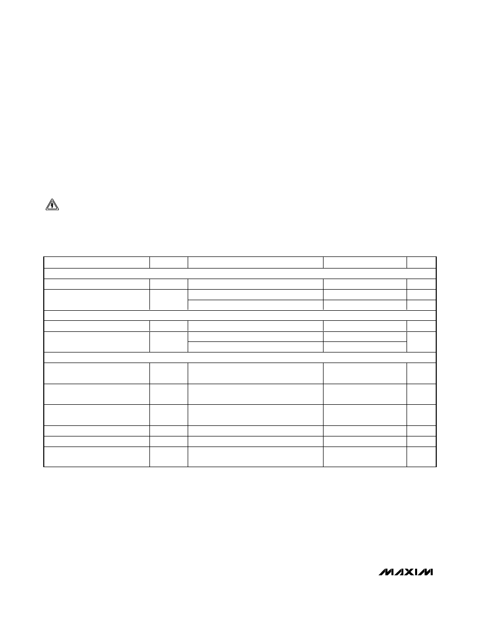
ABSOLUTE MAXIMUM RATINGS
DC ELECTRICAL CHARACTERISTICS
(MAX3580 EV kit, V
CC
= +3.1V to +3.5V, GND = 0V, BB_AGC = RF_AGC = +2.85V, RF input terminated into a 75Ω load, BBI_ and
BBQ_ are open, no input signal, VCO active, registers set according to the specified default register conditions, T
A
= -40°C to
+85°C, unless otherwise specified. Typical values are at V
CC
= +3.3V, T
A
=+25°C, unless otherwise specified.) (Note 1)
Stresses beyond those listed under “Absolute Maximum Ratings” may cause permanent damage to the device. These are stress ratings only, and functional
operation of the device at these or any other conditions beyond those indicated in the operational sections of the specifications is not implied. Exposure to
absolute maximum rating conditions for extended periods may affect device reliability.
V
CC
to GND ...........................................................-0.3V to +3.6V
SDA, SCL, ADDR2, MUX, REF_BUFF,
BB_AGC, RF_AGC to GND ................................-0.3V to +3.6V
All Other Pins to GND ..............................-0.3V to (+V
CC
+ 0.3V)
RF Input Power ...............................................................+10dBm
Operating Temperature Range ...........................-40°C to +85°C
Junction Temperature ......................................................+150°C
Storage Temperature Range .............................-65°C to +165°C
Continuous Power Dissipation (T
A
= +70°C)
(derate 21.3mW/°C above +70°C) ..............................1702mW
Lead Temperature (soldering, 10s) .................................+300°C
PARAMETER
SYMBOL
CONDITIONS
MIN
TYP
MAX
UNITS
SUPPLY VOLTAGE AND CURRENT
Supply Voltage
V
CC
3.1
3.5
V
Active
197
225
mA
Supply Current
I
CC
Shutdown mode
200
µA
RF_AGC AND BB_AGC
Input Bias Current
I
AGC
V
AGC
at +0.5V and +2.85V
-50
+50
µA
Maximum gain
2.85
RF and Baseband AGC Control
Voltage
V
AGC
Minimum gain
0.5
V
SERIAL INTERFACE AND MUX OUTPUT (SCL, SDA, MUX)
Input Logic-Level Low
V
IL
0.3 x
V
CC
V
Input Logic-Level High
V
IH
0.7 x
V
CC
V
Input Hysteresis
0.05 x
V
CC
V
SDA, SCL Input Current
-10
+10
µA
Output Logic-Level Low
V
OL
Sink current = 0.3mA
0.4
V
Output Logic-Level High
V
OH
Source current = 0.3mA
V
CC
-
0.5
V
CAUTION! ESD SENSITIVE DEVICE