Max3580 direct-conversion tv tuner, Pin description – Rainbow Electronics MAX3580 User Manual
Page 10

MAX3580
Direct-Conversion TV Tuner
10
______________________________________________________________________________________
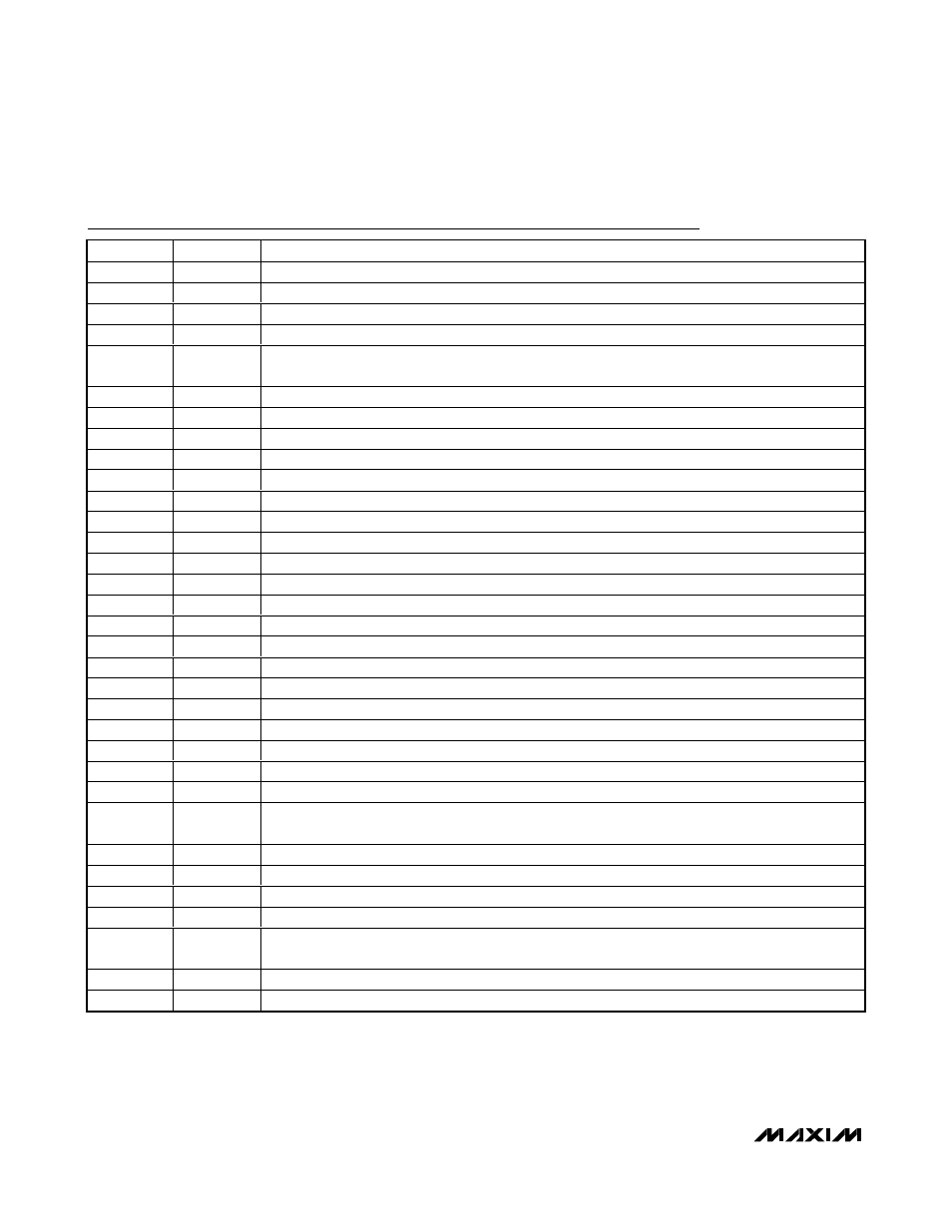
Pin Description
PIN
NAME
FUNCTION
1
SDA
Serial-Data Input Line. Requires a pullup resistor to V
CC
.
2
SCL
Serial-Clock Input. Requires a pullup resistor to V
CC
.
3
RFIN2
Second RF Input
4
RFIN
First RF Input
5
ADDR2
Address Line. Sets the 3rd LSB of the device address. Connect to ground to set for “0” or V
CC
to set
for “1.”
6
GND_LNA
Not Internally Connected. Connect to ground.
7
VCC_RF
DC Supply for RF LNA. Connect as close as possible a 100pF capacitor from this pin to GND.
8
LEXT
External Bias Inductor. Connect to V
CC
with a 270nH inductor.
9
RF_AGC
Gain Control Input for RF VGA.
10
IND1
VHF Inductor Pin 1. Keep traces to inductor as short as possible.
11
IND2
VHF Inductor Pin 2. Keep traces to inductor as short as possible.
12
N.C.
No Connection
13
OVLD_DET
Overload Detector Output. Connect a 10k
Ω pullup resistor to V
CC
and a RC network to RF_AGC.
14
VCC_BB
D C S up p l y for Baseb and Fi l ter . C onnect as cl ose as p ossi b l e a 10nF cap aci tor fr om thi s p i n to g r ound .
15
BBQ-
Quadrature Inverted Baseband Output
16
BBQ+
Quadrature Noninverted Baseband Output
17
BBI-
In-Phase, Inverted Baseband Output
18
BBI+
In-Phase, Noninverted Baseband Output
19
BB_AGC
Gain Control Input for Baseband VGAs
20
VCC_VCO
DC Supply for the VCO. Connect as close as possible a 100pF capacitor from this pin to ground.
21
VTUNE
VCO Tuning Voltage Input. Connect the PLL loop filter output directly to this pin.
22
GND_TUNE
Ground Reference for the Tuning Voltage. Connect to ground of the loop filter.
23
LDO
VCO LDO Output. Connect a 0.1µF capacitor to ground.
24
CP
Charge-Pump Output. Connect the charge-pump output to the PLL loop filter input.
25
GND_CP
Ground for the Charge Pump
26
VCC_SYN
DC Supply for Synthesizer and Serial-Interface Control. Connect as close as possible a 10nF
capacitor from this pin to ground.
27
GND_PLL
Ground for the PLL
28
MUX
Multiplex Output Line. Can be used as a PLL lock-detector output.
29
REF_BUFF
Buffered Output of Reference Oscillator
30
VCC_XTAL
D C S up p l y for Refer ence Osci l l ator . C onnect as cl ose as p ossi b l e a 10nF cap aci tor fr om thi s p i n to g r ound .
31
XB
Reference Input. Connect to a parallel resonant mode XTAL through a load-matching capacitor, or
can also be used as a reference clock input pin.
32
XE
Reference Oscillator Feedback. Connect to a capacitive divider when used in self-oscillating mode.
EP
EP
Exposed Paddle. Solder to the board’s ground plane to achieve the lowest possible impedance path.
