Electrical characteristics (continued) – Rainbow Electronics MAX1182 User Manual
Page 5
MAX1182
Dual 10-Bit, 65Msps, +3V, Low-Power ADC with
Internal Reference and Parallel Outputs
_______________________________________________________________________________________
5
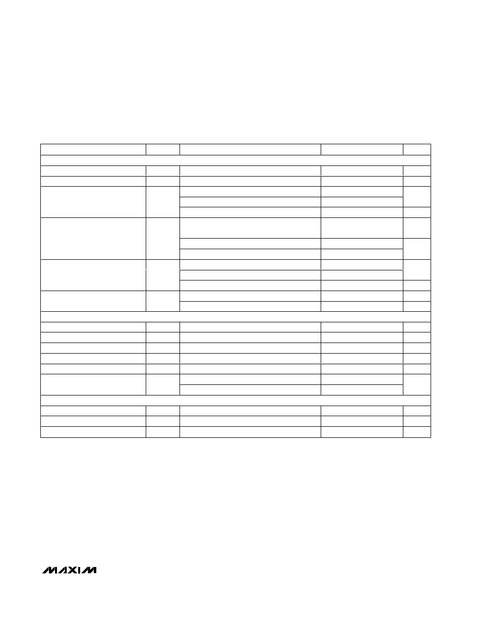
ELECTRICAL CHARACTERISTICS (continued)
(V
DD
= +3V, OV
DD
= +2.5V; 0.1µF and 1.0µF capacitors from REFP, REFN, and COM to GND; REFOUT connected to REFIN through
a 10k
Ω resistor, V
IN
= 2Vp-p (differential w.r.t. COM), C
L
= 10pF at digital outputs (Note 5), f
CLK
= 65MHz (50% duty cycle),
T
A
= T
MIN
to T
MAX
, unless otherwise noted. Typical values are at T
A
= +25°C.)
PARAMETER
SYMBOL
CONDITIONS
MIN
TYP
MAX
UNITS
POWER REQUIREMENTS
Analog Supply Voltage Range
V
DD
2.7
3.0
3.6
V
Output Supply Voltage Range
OV
DD
1.7
2.5
3.6
V
Operating, f
INA or B
= 20MHz at -0.5dB FS
65
80
Sleep mode
2.8
mA
Analog Supply Current
I
VDD
Shutdown, clock idle, PD =
OE = OV
DD
1
15
µA
Operating, C
L
= 15pF, f
INA or B
= 20MHz at
-0.5dB FS
11
mA
Sleep mode
100
Output Supply Current
I
OVDD
Shutdown, clock idle, PD =
OE = OV
DD
2
10
µA
Operating, f
INA or B
= 20MHz at -0.5dB FS
195
240
Sleep mode
8.4
mW
Power Dissipation
PDISS
Shutdown, clock idle, PD =
OE = OV
DD
3
45
µW
Offset
±0.2
mV/V
Power-Supply Rejection Ratio
PSRR
Gain
±0.1
%/V
TIMING CHARACTERISTICS
CLK Rise to Output Data Valid
t
DO
Figure 3 (Note 3)
5
8
ns
Output Enable Time
t
ENABLE
Figure 4
10
ns
Output Disable Time
t
DISABLE
Figure 4
1.5
ns
CLK Pulse Width High
t
CH
Figure 3, clock period: 15.4ns
7.7
± 1.5
ns
CLK Pulse Width Low
t
CL
Figure 3, clock period: 15.4ns
7.7
± 1.5
ns
Wakeup from Sleep mode (Note 4)
0.42
Wake-Up Time
t
WAKE
Wakeup from Shutdown (Note 4)
1.5
µs
CHANNEL-TO-CHANNEL MATCHING
Crosstalk
f
INA or B
= 20MHz at -0.5dB FS
-70
dB
Gain Matching
f
INA or B
= 20MHz at -0.5dB FS
0.02
±0.2
dB
Phase Matching
f
INA or B
= 20MHz at -0.5dB FS
0.25
d eg r ees
Note 1: SNR, SINAD, THD, SFDR, and HD3 are based on an analog input voltage of -0.5dB FS referenced to a +1.024V full-scale
input voltage range.
Note 2: Intermodulation distortion is the total power of the intermodulation products relative to the individual carrier. This number is
6dB or better, if referenced to the two-tone envelope.
Note 3: Digital outputs settle to V
IH
, V
IL
. Parameter guaranteed by design.
Note 4: With REFIN driven externally, REFP, COM, and REFN are left floating while powered down.
Note 5: Equivalent dynamic performance is obtainable over full OV
DD
range with reduced C
L
.