Electrical characteristics (continued) – Rainbow Electronics MAX1182 User Manual
Page 3
MAX1182
Dual 10-Bit, 65Msps, +3V, Low-Power ADC with
Internal Reference and Parallel Outputs
_______________________________________________________________________________________
3
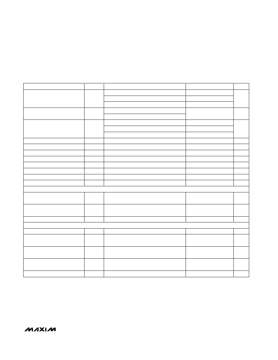
ELECTRICAL CHARACTERISTICS (continued)
(V
DD
= +3V, OV
DD
= +2.5V; 0.1µF and 1.0µF capacitors from REFP, REFN, and COM to GND; REFOUT connected to REFIN through
a 10k
Ω resistor, V
IN
= 2Vp-p (differential w.r.t. COM), C
L
= 10pF at digital outputs (Note 5), f
CLK
= 65MHz (50% duty cycle),
T
A
= T
MIN
to T
MAX
, unless otherwise noted. Typical values are at T
A
= +25°C.)
PARAMETER
SYMBOL
CONDITIONS
MIN
TYP
MAX
UNITS
f
INA or B
= 7.47MHz
-83
f
INA or B
= 20MHz
-82
Third-Harmonic Distortion
HD3
f
INA or B
= 39.9MHz (Note 1)
-77
dBc
f
INA or B
= 19.13042MHz at -6.5dB FS
Intermodulation Distortion
(first 5 odd-order IMDs)
IMD
f
I N A o r B
= 21.2886M H z at - 6.5d B FS ( N ote 2)
-75
dBc
f
INA or B
= 7.47MHz, T
A
= +25
°C
-75.5
-64
f
INA or B
= 20MHz, T
A
= +25
°C
-76
-63
Total Harmonic Distortion
(first 5 harmonics)
THD
f
INA or B
= 39.9MHz, (Note 1)
-74
dBc
Small-Signal Bandwidth
Input at -20dB FS, differential inputs
500
MHz
Full-Power Bandwidth
FPBW
Input at -0.5dB FS, differential inputs
400
MHz
Aperture Delay
t
AD
1
ns
Aperture Jitter
t
AJ
2
ps
RMS
Overdrive Recovery Time
For 1.5 x full-scale input
2
ns
Differential Gain
±1
%
Differential Phase
±0.25
d egr ees
Output Noise
INA+ = INA- = INB+ = INB- = COM
0.2
LSB
RMS
INTERNAL REFERENCE
Reference Output Voltage
REFOUT
2.048
±3%
V
Reference Temperature
Coefficient
TC
REF
60
ppm/
°C
Load Regulation
1.25
mV/mA
BUFFERED EXTERNAL REFERENCE (V
REFIN
= +2.048V)
REFIN Input Voltage
V
REFIN
2.048
V
Positive Reference Output
Voltage
V
REFP
2.012
V
Negative Reference Output
Voltage
V
REFN
0.988
V
Differential Reference Output
Voltage Range
∆V
REF
∆V
REF
= V
REFP
- V
REFN
0.98
1.024
1.07
V
REFIN Resistance
R
REFIN
>50
M
Ω