Grounding, bypassing, and board layout – Rainbow Electronics MAX1182 User Manual
Page 15
MAX1182
Dual 10-Bit, 65Msps, +3V, Low-Power ADC with
Internal Reference and Parallel Outputs
______________________________________________________________________________________
15
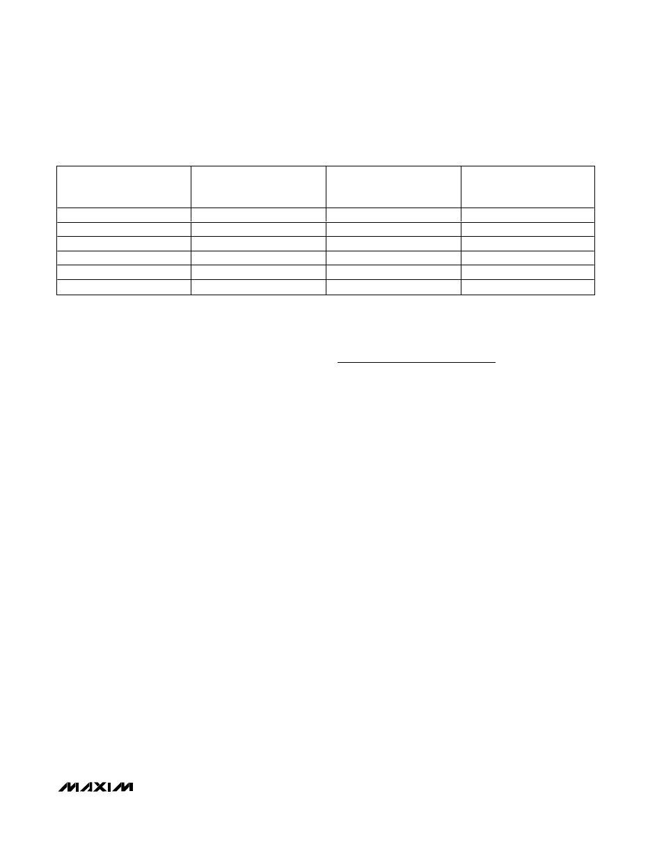
Table 1. MAX1182 Output Codes For Differential Inputs
*V
REF
= V
REFP
- V
REFN
DIFFERENTIAL INPUT
VOLTAGE*
DIFFERENTIAL
INPUT
STRAIGHT OFFSET
BINARY
T/B = 0
TWO’S COMPLEMENT
T/B = 1
V
REF
x 511/512
+FULL SCALE - 1LSB
11 1111 1111
01 1111 1111
V
REF
x 1/512
+ 1 LSB
10 0000 0001
00 0000 0001
0
Bipolar Zero
10 0000 0000
00 0000 0000
- V
REF
x 1/512
- 1 LSB
01 1111 1111
11 1111 1111
-V
REF
x 511/512
- FULL SCALE + 1 LSB
00 0000 0001
10 0000 0001
-V
REF
x 512/512
- FULL SCALE
00 0000 0000
10 0000 0000
Single-Ended AC-Coupled Input Signal
Figure 7 shows an AC-coupled, single-ended applica-
tion. Amplifiers like the MAX4108 provide high-speed,
high-bandwidth, low noise, and low distortion to main-
tain the integrity of the input signal.
Typical QAM Demodulation Application
The most frequently used modulation technique for dig-
ital communications applications is probably the
Quadrature Amplitude Modulation (QAM). Typically
found in spread-spectrum based systems, a QAM sig-
nal represents a carrier frequency modulated in both
amplitude and phase. At the transmitter, modulating the
baseband signal with quadrature outputs, a local oscil-
lator followed by subsequent up-conversion can gener-
ate the QAM signal. The result is an in-phase (I) and a
quadrature (Q) carrier component, where the Q compo-
nent is 90 degree phase-shifted with respect to the in-
phase component. At the receiver, the QAM signal is
divided down into it’s I and Q components, essentially
representing the modulation process reversed. Figure 8
displays the demodulation process performed in the
analog domain, using the dual matched +3V, 10-bit
ADC MAX1182 and the MAX2451 quadrature demodu-
lator to recover and digitize the I and Q baseband sig-
nals. Before being digitized by the MAX1182, the
mixed-down signal components may be filtered by
matched analog filters, such as Nyquist or pulse-shap-
ing filters which remove any unwanted images from the
mixing process, thereby enhancing the overall signal-
to-noise (SNR) performance and minimizing inter-sym-
bol interference.
Grounding, Bypassing, and
Board Layout
The MAX1182 requires high-speed board layout design
techniques. Locate all bypass capacitors as close to
the device as possible, preferably on the same side as
the ADC, using surface-mount devices for minimum
inductance. Bypass V
DD
, REFP, REFN, and COM with
two parallel 0.1µF ceramic capacitors and a 2.2µF
bipolar capacitor to GND. Follow the same rules to
bypass the digital supply (OV
DD
) to OGND. Multilayer
boards with separated ground and power planes pro-
duce the highest level of signal integrity. Consider the
use of a split ground plane arranged to match the
physical location of the analog ground (GND) and the
digital output driver ground (OGND) on the ADCs pack-
age. The two ground planes should be joined at a sin-
gle point such that the noisy digital ground currents do
not interfere with the analog ground plane. The ideal
location of this connection can be determined experi-
mentally at a point along the gap between the two
ground planes, which produces optimum results. Make
this connection with a low-value, surface-mount resistor
(1
Ω to 5Ω), a ferrite bead or a direct short. Alternatively,
all ground pins could share the same ground plane, if
the ground plane is sufficiently isolated from any noisy,
digital systems ground plane (e.g., downstream output
buffer or DSP ground plane). Route high-speed digital
signal traces away from the sensitive analog traces of
either channel. Make sure to isolate the analog input
lines to each respective converter to minimize channel-
to-channel crosstalk. Keep all signal lines short and
free of 90 degree turns.