Applications information – Rainbow Electronics MAX1182 User Manual
Page 14
MAX1182
Dual 10-Bit, 65Msps, +3V, Low-Power ADC with
Internal Reference and Parallel Outputs
14
______________________________________________________________________________________
Applications Information
Figure 5 depicts a typical application circuit containing
two single-ended to differential converters. The internal
reference provides a V
DD
/2 output voltage for level
shifting purposes. The input is buffered and then split to
a voltage follower and inverter. One lowpass filter per
ADC suppresses some of the wideband noise associat-
ed with high-speed operational amplifiers, follows the
amplifiers. The user may select the R
ISO
and C
IN
val-
ues to optimize the filter performance, to suit a particu-
lar application. For the application in Figure 5, a R
ISO
of
50
Ω is placed before the capacitive load to prevent
ringing and oscillation. The 22pF C
IN
capacitor acts as
a small bypassing capacitor.
Using Transformer Coupling
A RF transformer (Figure 6) provides an excellent solu-
tion to convert a single-ended source signal to a fully
differential signal, required by the MAX1182 for opti-
mum performance. Connecting the center tap of the
transformer to COM provides a V
DD
/2 DC level shift to
the input. Although a 1:1 transformer is shown, a step-
up transformer may be selected to reduce the drive
requirements. A reduced signal swing from the input
driver, such as an op amp, may also improve the over-
all distortion.
In general, the MAX1182 provides better SFDR and
THD with fully-differential input signals than single-
ended drive, especially for very high input frequencies.
In differential input mode, even-order harmonics are
lower as both inputs (INA+, INA- and/or INB+, INB-) are
balanced, and each of the ADC inputs only requires
half the signal swing compared to single-ended mode.
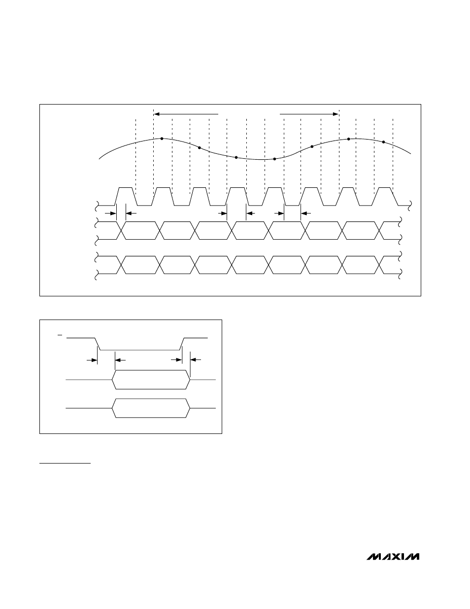
N - 6
N
N - 5
N + 1
N - 4
N + 2
N - 3
N + 3
N - 2
N + 4
N - 1
N + 5
N
N + 6
N + 1
5 CLOCK-CYCLE LATENCY
ANALOG INPUT
CLOCK INPUT
DATA OUTPUT
D9A–D0A
t
D0
t
CH
t
CL
N - 6
N - 5
N - 4
N - 3
N - 2
N - 1
N
N + 1
DATA OUTPUT
D9B–D0B
OUTPUT
D9A–D0A
OE
t
DISABLE
t
ENABLE
HIGH-Z
HIGH-Z
VALID DATA
OUTPUT
D9B–D0B
HIGH-Z
HIGH-Z
VALID DATA
Figure 3. System Timing Diagram
Figure 4. Output Timing Diagram