Electrical characteristics (continued) – Rainbow Electronics MAX1182 User Manual
Page 4
MAX1182
Dual 10-Bit, 65Msps, +3V, Low-Power ADC with
Internal Reference and Parallel Outputs
4
_______________________________________________________________________________________
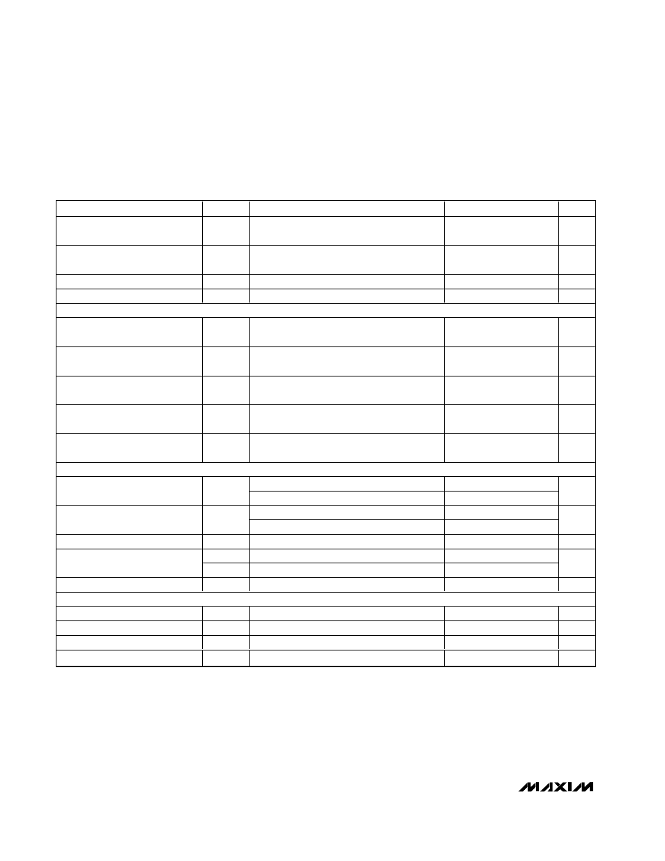
ELECTRICAL CHARACTERISTICS (continued)
(V
DD
= +3V, OV
DD
= +2.5V; 0.1µF and 1.0µF capacitors from REFP, REFN, and COM to GND; REFOUT connected to REFIN through
a 10k
Ω resistor, V
IN
= 2Vp-p (differential w.r.t. COM), C
L
= 10pF at digital outputs (Note 5), f
CLK
= 65MHz (50% duty cycle),
T
A
= T
MIN
to T
MAX
, unless otherwise noted. Typical values are at T
A
= +25°C.)
PARAMETER
SYMBOL
CONDITIONS
MIN
TYP
MAX
UNITS
Maximum REFP, COM Source
Current
I
SOURCE
>5
mA
Maximum REFP, COM Sink
Current
I
SINK
250
µA
Maximum REFN Source Current
I
SOURCE
250
µA
Maximum REFN Sink Current
I
SINK
>5
mA
UNBUFFERED EXTERNAL REFERENCE (V
REFIN
= AGND, reference voltage applied to REFP, REFN, and COM)
REFP, REFN Input Resistance
R
REFP
,
R
REFN
Measured between REFP and COM, and
REFN and COM
4
k
Ω
Differential Reference Input
Voltage
∆V
REF
∆V
REF
= V
REFP
– V
REFN
1.024
±10%
V
COM Input Voltage
V
COM
VDD/2
± 10%
V
REFP Input Voltage
V
REFP
V
COM
+
∆V
REF
/2
V
REFN Input Voltage
V
REFN
V
COM
-
∆V
REF
/2
V
DIGITAL INPUTS (CLK, PD, OE, SLEEP, T/B)
CLK
0.8 x V
DD
Input High Threshold
V
IH
PD, OE, SLEEP, T/B
0.8 x OV
DD
V
CLK
0.2 x V
DD
Input Low Threshold
V
IL
PD, OE, SLEEP, T/B
0.2 x OV
DD
V
Input Hysteresis
V
HYST
0.1
V
I
IH
V
IH
= OV
DD
or V
DD
(CLK)
±5
Input Leakage
I
IL
V
IL
= 0
±5
µA
Input Capacitance
C
IN
5
pF
DIGITAL OUTPUTS (D9A–D0A, D9B–D0B)
Output Voltage Low
V
OL
I
SINK
= 200µA
0.2
V
Output Voltage High
V
OH
I
SOURCE
= 200µA
OV
DD
- 0.2
V
Three-State Leakage Current
I
LEAK
OE = OV
DD
±10
µA
Three-State Output Capacitance
C
OUT
OE = OV
DD
5
pF