Typical operating characteristics, Electrical characteristics (continued) – Rainbow Electronics MAX1301 User Manual
Page 6
MAX1300/MAX1301
8-/4-Channel, ±12V Multirange Inputs,
Serial 16-Bit ADCs
6
_______________________________________________________________________________________
PARAMETER
SYMBOL
CONDITIONS
MIN
TYP
MAX
UNITS
CS Rise to DOUT Disable
t
TR
40
ns
CS Fall to SCLK Rise Setup
t
CSS
40
ns
CS High Minimum Pulse Width
t
CSPW
40
ns
SCLK Fall to CS Rise Hold
t
CSH
0
ns
SSTRB Rise to CS Fall Setup
(Note 4)
40
ns
DOUT Rise/Fall Time
C
L
= 50pF
10
ns
SSTRB Rise/Fall Time
C
L
= 50pF
10
ns
Note 1: Parameter tested at AV
DD1
= AV
DD2
= DV
DD
= DV
DDO
= 5V.
Note 2: See definitions in the Parameter Definitions section at the end of the data sheet.
Note 3: Guaranteed by correlation with single-ended measurements.
Note 4: Not production tested. Guaranteed by design.
Note 5: To ensure external reference operation, V
REFCAP
must exceed (AV
DD1
- 0.1V). To ensure internal reference operation, V
REFCAP
must be below (AV
DD1
- 0.4V). Bypassing REFCAP with a 0.1µF or larger capacitor to AGND1 sets VREFCAP
≈ 4.096V. The tran-
sition point between internal reference mode and external reference mode lies between the REFCAP buffer disable threshold
minimum and maximum values (Figures 17 and 18).
Note 6: The SCLK duty cycle can vary between 40% and 60%, as long as the t
CL
and t
CH
timing requirements are met.
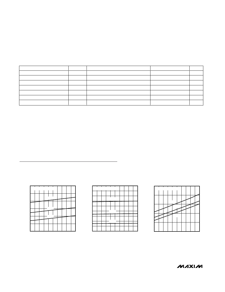
ANALOG SUPPLY CURRENT
vs. ANALOG SUPPLY VOLTAGE
MAX1300/01 toc01
AV
DD1
(V)
I
AVDD1
(mA)
5.15
5.05
4.95
4.85
2.35
2.40
2.45
2.50
2.55
2.60
2.30
4.75
5.25
+85
°C
+25
°C
-40
°C
EXTERNAL CLOCK MODE
PREAMPLIFIER SUPPLY CURRENT
vs. PREAMPLIFIER SUPPLY VOLTAGE
MAX1300/01 toc02
AV
DD2
(V)
I
AVDD2
(mA)
5.15
5.05
4.85
4.95
16
17
18
19
20
21
22
23
24
15
4.75
5.25
+85
°C
+25
°C
-40
°C
EXTERNAL CLOCK MODE
DIGITAL SUPPLY CURRENT
vs. DIGITAL SUPPLY VOLTAGE
MAX1300/01 toc03
DV
DD
(V)
I
DVDD
(mA)
5.15
5.05
4.95
4.85
0.70
0.75
0.80
0.85
0.90
0.65
4.75
5.25
+85
°C
+25
°C
-40
°C
EXTERNAL CLOCK MODE
Typical Operating Characteristics
(AV
DD1
= AV
DD2
= DV
DD
= DV
DDO
= 5V, AGND1 = DGND = DGNDO = AGND2 = AGND3 = 0, f
CLK
= 3.5MHz (50% duty cycle),
external clock mode, V
REF
= 4.096V (external reference operation), REFCAP = AV
DD1
, maximum single-ended bipolar input range,
C
DOUT
= 50pF, C
SSTRB
= 50pF; unless otherwise noted.)
ELECTRICAL CHARACTERISTICS (continued)
(AV
DD1
= AV
DD2
= DV
DD
= DV
DDO
= 5V, AGND1 = DGND = DGNDO = AGND2 = AGND3 = 0, f
CLK
= 3.5MHz (50% duty cycle),
external clock mode, V
REF
= 4.096V (external reference operation), REFCAP = AV
DD1
, maximum single-ended bipolar input range
(±12V), C
DOUT
= 50pF, C
SSTRB
= 50pF, T
A
= -40°C to +85°C, unless otherwise noted. Typical values are at T
A
= +25°C.)