Rainbow Electronics MAX1301 User Manual
Page 21

Start Bit
Communication with the MAX1300/MAX1301 is accom-
plished using the three input data word formats shown
in Table 3. Each input data word begins with a start bit.
The start bit is defined as the first high bit clocked into
DIN with CS low when any of the following are true:
• Data conversion is not in process and all data from
the previous conversion has clocked out of DOUT.
• The device is configured for operation in external
clock mode (mode 0) and previous conversion-result
bits B15–B3 have clocked out of DOUT.
• The device is configured for operation in external
acquisition mode (mode 1) and previous conversion-
result bits B15–B7 have clocked out of DOUT.
• The device is configured for operation in internal
clock mode, (mode 2) and previous conversion-
result bits B15–B4 have clocked out of DOUT.
Output Data Format
Output data is clocked out of DOUT in offset binary for-
mat on the falling edge of SCLK, MSB first (B15). For
output binary codes, see the Transfer Function section
and Figures 12, 13, and 14.
Configuring Analog Inputs
Each analog input has two configurable parameters:
• Single-ended or true-differential input
• Input voltage range
These parameters are configured using the analog input
configuration byte as shown in Table 2. Each analog
input has a dedicated register to store its input configura-
tion information. The timing diagram of Figure 15 shows
how to write to the analog input configuration registers.
Figure 16 shows DOUT and SSTRB timing.
Transfer Function
An ADC’s transfer function defines the relationship
between the analog input voltage and the digital output
code. Figures 12, 13, and 14 show the MAX1300/
MAX1301 transfer functions. The transfer function is
determined by the following characteristics:
• Analog input voltage range
• Single-ended or differential configuration
• Reference voltage
The axes of an ADC transfer function are typically in least
significant bits (LSBs). For the MAX1300/MAX1301, an
LSB is calculated using the following equation:
where N is the number of bits (N = 16) and FSR is the
full-scale range (see Figures 7 and 8).
1
2
4 096
.
LSB
FSR
V
V
REF
N
=
Ч
Ч
MAX1300/MAX1301
8-/4-Channel, ±12V Multirange Inputs,
Serial 16-Bit ADCs
______________________________________________________________________________________
21
INPUT VOLTAGE (V)
COMMON-MODE VOLTAGE (V)
12
6
0
-6
-12
-12
-8
-4
0
4
8
12
-16
-18
18
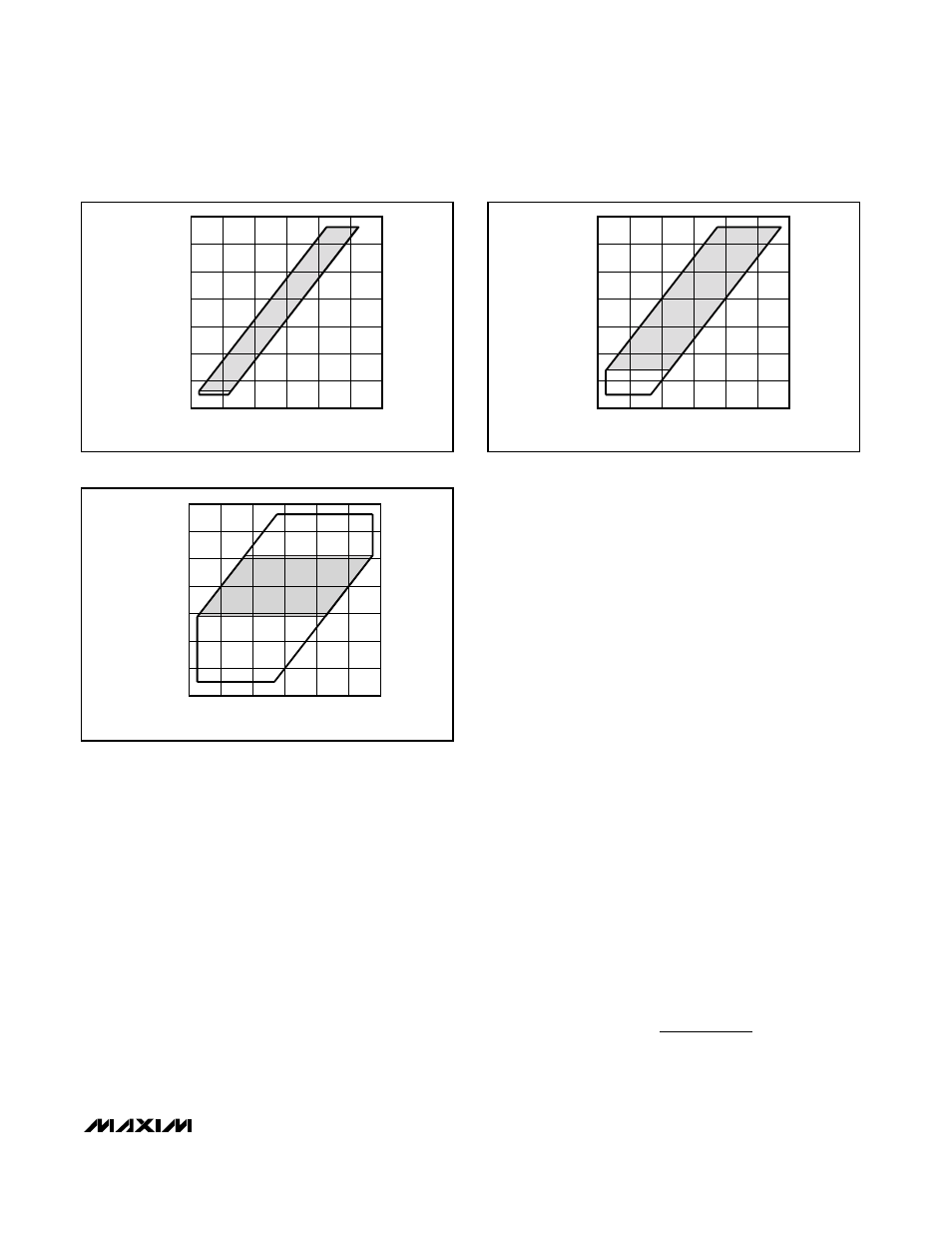
Figure 9. Common-Mode Voltage vs. Input Voltage (FSR = 12V)
INPUT VOLTAGE (V)
COMMON-MODE VOLTAGE (V)
12
6
0
-6
-12
-12
-8
-4
0
4
8
12
-16
-18
18
Figure 10. Common-Mode Voltage vs. Input Voltage (FSR = 24V)
INPUT VOLTAGE (V)
COMMON-MODE VOLTAGE (V)
12
6
0
-6
-12
-12
-8
-4
0
4
8
12
-16
-18
18
Figure 11. Common-Mode Voltage vs. Input Voltage (FSR = 48V)
