Pin description, Standard application circuit – Rainbow Electronics MAX1636 User Manual
Page 8
MAX1636
Low-Voltage, Precision Step-Down
Controller for Portable CPU Power
8
_______________________________________________________________________________________
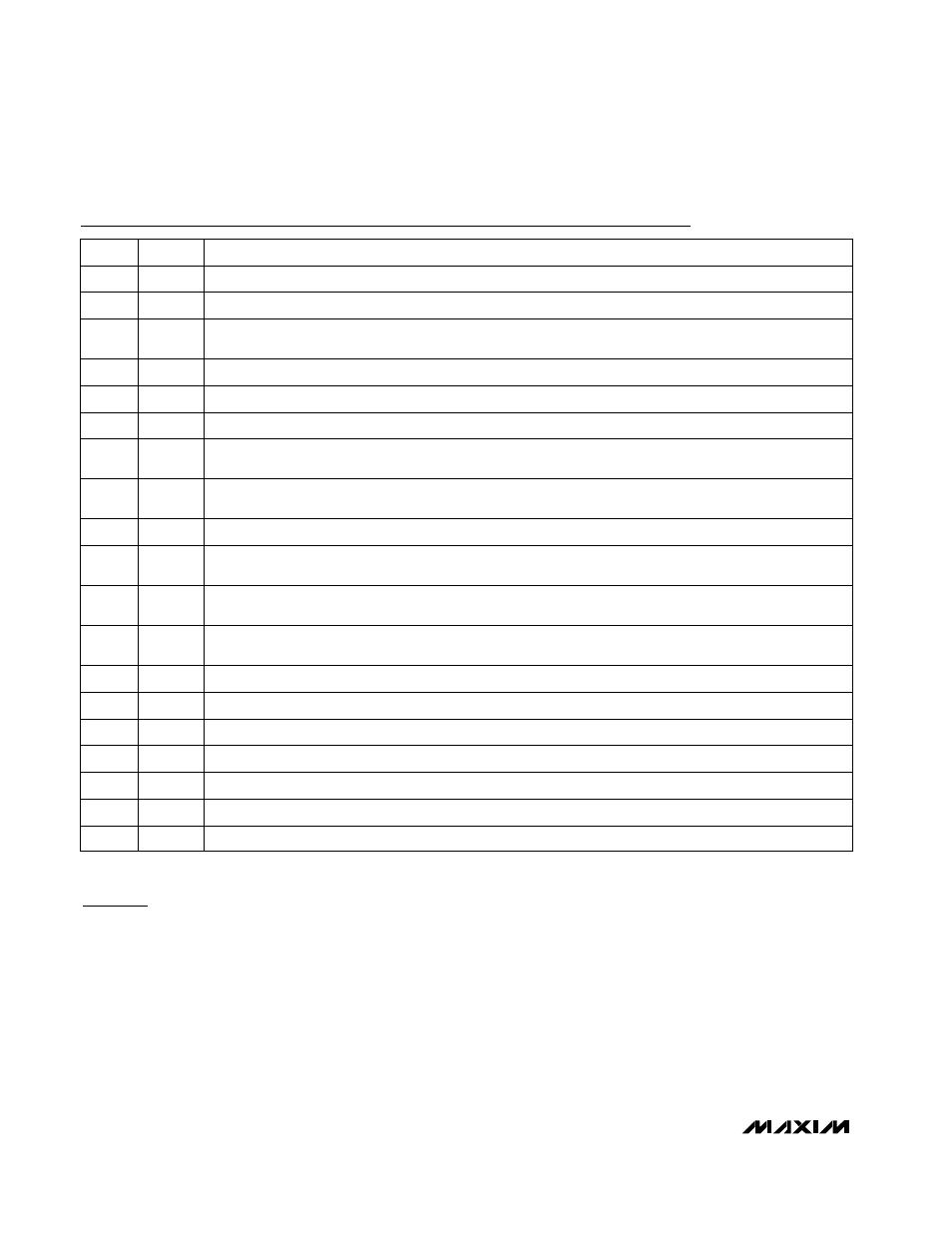
Pin Description
NAME
FUNCTION
1
CSH
Current-Sense Input, High Side
2
CSL
Current-Sense Input, Low Side. Also serves as a feedback input in fixed output modes.
PIN
3
RESET
Timed Reset Output. Low for at least 100ms after output voltage is valid, then goes high impedance
(open drain).
4
SHDN
Shutdown Control Input. Puts chip in shutdown or standby mode, depending on OVP (Table 5).
8
SYNC
Oscillator Frequency Select and Synchronization Input. Tie to V
CC
for 300kHz operation; tie to GND for
200kHz operation.
7
REF
1.100V Reference Output. Capable of sourcing 50µA for external loads; bypass with a 0.22µF
(min) capacitor.
6
CC
Compensation pin. Connect a small capacitor to GND to set the integration time constant.
5
OVP
Overvoltage Protection Enable/Disable. Tie to GND to disable OVP; tie to V
CC
to enable OVP.
13
V+
5V VL Linear-Regulator Input. The VL linear regulator automatically shuts off if V+ is shorted to V
L
. Bypass
V+ to GND with a 0.1µF capacitor close to the IC.
12
V
CC
Main Supply Voltage Input. Powers the PWM controller, logic, and reference. Input range is +3.15V to
+5.5V.
11
FB
Feedback Input. Tie to GND for fixed 3.3V output; tie to V
CC
for fixed 2.5V output; tie to resistor divider for
adjustable mode.
9, 10
GND
Analog Ground
15
DL
Low-Side Gate-Driver Output
14
VL
5V Linear-Regulator Output. Powers the DL low-side gate driver. Bypass with a 2.2µF (min) capacitor.
20
SKIP
Low-Noise Mode Control. Forces fixed-frequency PWM operation when high.
19
LX
Inductor Connection
18
DH
High-Side Gate-Driver Output
17
BST
Boost-Capacitor Connection
16
PGND
Power Ground
Standard Application Circuit
The basic MAX1636 buck converter (Figure 1) is easily
adapted to meet a wide range of applications with
inputs up to 30V by substituting components from
Table 1. These circuits represent a good set of trade-
offs between cost, size, and efficiency, while staying
within the worst-case specification limits for stress-
related parameters, such as capacitor ripple current.
Do not change the circuits’ switching frequency without
first recalculating component values (particularly induc-
tance value at maximum battery voltage). Adding a
Schottky rectifier across the synchronous rectifier
improves circuit efficiency by approximately 1%. This
rectifier is otherwise not needed because the MOSFET
required typically incorporates a high-speed silicon
diode from drain to source. Use a Schottky rectifier
rated at a DC current equal to at least one-third of the
load current.