Max1636, Chip information – Rainbow Electronics MAX1636 User Manual
Page 22

MAX1636
connections, the bottom layer for quiet connections
(REF, CC, GND), and the inner layers for an uninter-
rupted ground plane. Use the following step-by-step
guide:
1) Place the high-power components (C1, C2, Q1, Q2,
D1, L1, and R1) first, with their grounds adjacent.
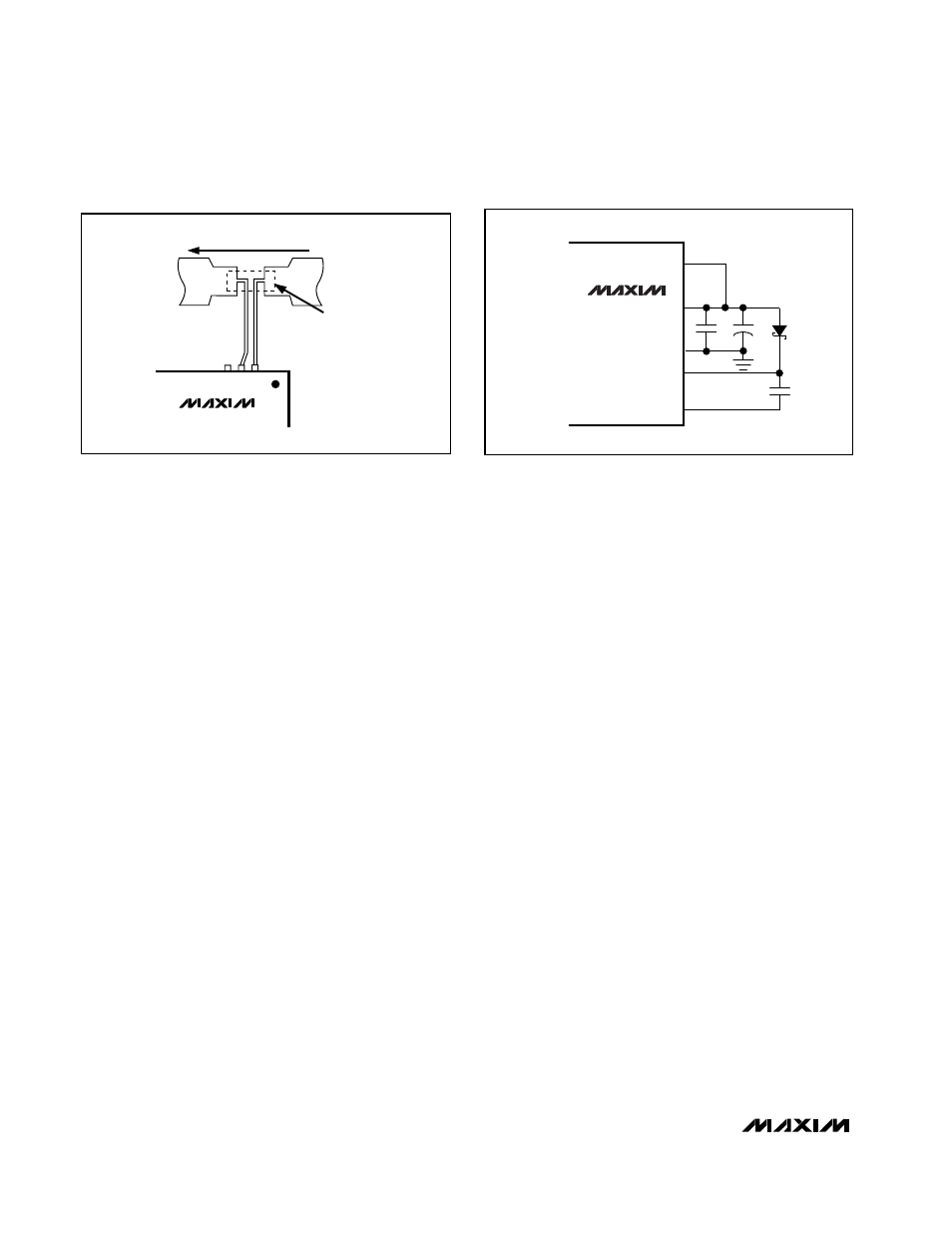
• Minimize current-sense resistor trace lengths and
ensure accurate current sensing with Kelvin con-
nections (Figure 6).
• Minimize ground trace lengths in the high-current
paths.
• Minimize other trace lengths in the high-current
paths.
— Use >5mm-wide traces.
— CIN to high-side MOSFET drain: 10mm
max length
— Rectifier diode cathode to low side
— MOSFET: 5mm max length
— LX node (MOSFETs, rectifier cathode, induc-
tor): 15mm max length
Ideally, surface-mount power components are butted
up to one another with their ground terminals almost
touching. These high-current grounds are then con-
nected to each other with a wide, filled zone of
top-layer copper so they do not go through vias. The
resulting top-layer subground plane is connected to the
normal inner-layer ground plane at the output ground
terminals, which ensures that the IC’s analog ground is
sensing at the supply’s output terminals without interfer-
ence from IR drops and ground noise. Other high-cur-
rent paths should also be minimized, but focusing
primarily on short ground and current-sense connec-
tions eliminates about 90% of all PC board layout prob-
lems (see the PC board layouts in the MAX1636
evaluation kit manual for examples).
2) Place the IC and signal components. Keep the main
switching nodes (LX nodes) away from sensitive
analog components (current-sense traces and REF
capacitor). Place the IC and analog components on
the opposite side of the board from the power-
switching node. Important: The IC must be no fur-
ther than 10mm from the current-sense resistors.
Keep the gate-drive traces (DH, DL, and BST) short-
er than 20mm and route them away from CSH, CSL,
and REF. Place ceramic bypass capacitors close to
the IC. The bulk capacitors can be placed further
away. If using VL to power V
CC
, minimize noise by
placing a 0.1µF capacitor close to the V
CC
pin and
placing the 4.7µF capacitor further away, but closer
than the boost diode (Figure 7).
3) Use a single-point star ground where the input
ground trace, power ground (subground plane), and
normal ground plane meet at the supply's output
ground terminal. Connect both IC ground pins and
all IC bypass capacitors to the normal ground plane.
Low-Voltage, Precision Step-Down
Controller for Portable CPU Power
22
______________________________________________________________________________________
MAX1636
SENSE RESISTOR
HIGH-CURRENT PATH
MAX1636
LX
VL
V
CC
GND
BST
Figure 6. Kelvin Connections for the Current-Sense Resistors
Figure 7. Capacitor Placement
TRANSISTOR COUNT: 3472
___________________Chip Information
