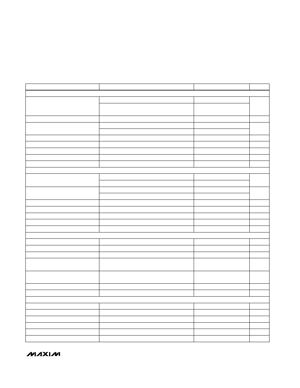
Electrical characteristics (continued) – Rainbow Electronics MAX1636 User Manual
Page 3

MAX1636
Low-Voltage, Precision Step-Down
Controller for Portable CPU Power
_______________________________________________________________________________________
3
ELECTRICAL CHARACTERISTICS (continued)
(Circuit of Figure 1, V+ = 15V, SYNC = VL = V
CC
, I
VL
= 0mA, I
REF
= 0mA, T
A
= 0°C to +85°C, unless otherwise noted. Typical values
are at T
A
= +25°C.)
%
FB to DL delay, 22mV overdrive, C
GATE
= 2000pF
SHDN = GND, OVP = V
CC
FB, with respect to regulation point
V
CC
= 5V, I(VL) = 0, V+ = 4.5V
(includes PNP base current)
V
CC
= 5V, I(VL) = 0
Guaranteed by design
SYNC = V
CC
SYNC = GND
SYNC = V
CC
I(VL) = 0 to 25mA, 5V < V+ < 30V
I(VL) = 0 to 25mA, 6V < V+ < 30V
Rising edge, hysteresis = 25mV
SYNC = GND
REF load = 0 to 50µA
SYNC = GND
°C
150
µs
1.25
%
4 7
10
kHz
240
340
SYNC Input Frequency Range
ns
200
SYNC Input Rise/Fall Time
ns
200
SYNC Input Pulse Width Low
200
Maximum Duty Factor, Dropout Mode
98
99
93
96
µA
60
Standby Supply Current (V+)
µA
500
Regulator Supply Current (V+)
60
91
94
170
200
230
270
300
330
kHz
V
4.5
5.0 5.3
4.7
5.0 5.3
VL Output Voltage
V
3.15
VL/ V
CC
Switchover Threshold
mV
10
REF Load Regulation
Hysteresis = 10°C
Rising edge, hysteresis = 25mV
V
3.45
3.60
3.75
VL Undervoltage Lockout Threshold
No REF load
V
1.090
1.100
1.110
REF Output Voltage
V
CC
= 3.3V to 5.5V
mV
3
REF Line Regulation
Oscillator Frequency
%
ns
SYNC Input Pulse Width High
Maximum Duty Factor
Overvoltage Trip Threshold
Thermal Shutdown Threshold
Overvoltage Fault Propagation Delay
%
Pin at GND or V
CC
; SKIP, OVP, SYNC
SHDN, SKIP, OVP, SYNC
SHDN, SKIP, OVP, SYNC
Falling edge (hysteresis = 1%)
From shutdown or power-on-reset state
% of nominal output
V
0.4
RESET Output Voltage Low
µA
-1
1
V
0.8
V
2.4
Logic Input Voltage High
clks
Catastrophic Output Undervoltage
Lockout Delay
Logic Input Voltage Low
Logic Input Bias Current
clks
32768
RESET Delay Time
%
-6 -3
RESET Trip Threshold
6144
Catastrophic Output Undervoltage
Lockout Threshold
60
70
80
I
SINK
= 4mA
+5.5V stress voltage applied
µA
1
RESET Output Leakage Current
CONDITIONS
UNITS
MIN
TYP
MAX
PARAMETER
SHDN = GND or V+
µA
-3
3
SHDN Input Bias Current
INTERNAL VL REGULATOR AND REFERENCE
OSCILLATOR
OVERVOLTAGE PROTECTION
INPUTS AND OUTPUTS
