Max1636 – Rainbow Electronics MAX1636 User Manual
Page 14

MAX1636
REF and VL Supplies and V
CC
Input
The 1.1V reference (REF) is accurate to ±1% over tem-
perature, making REF useful as a precision system ref-
erence. Bypass REF to GND with a 0.22µF (min)
capacitor. REF can supply up to 50µA for external
loads. Loading REF reduces the main output voltage
slightly because of the reference load-regulation error.
The 5V VL linear-regulator output can be tied to the
system +5V supply in order to obtain gate-drive power
from an efficient source. The two supply pins (V
CC
and
VL) are independent of each other (no protection
diodes or sequencing requirements), allowing you to
choose the most efficient sources for chip biasing from
among existing system supply voltages without having
to worry about sequencing or latch-up problems
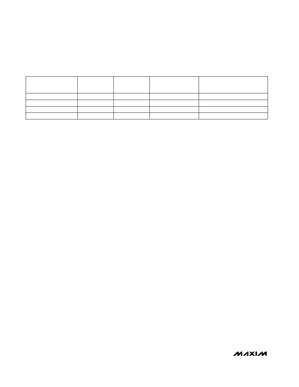
(Table 4).
The V
CC
input runs the chip if the V
CC
voltage is
greater than 3.15V. Otherwise, the chip supply is pow-
ered from VL via the internal V
CC
-VL switchover circuit.
If a system supply between 3.3V and 5V is not avail-
able, tie V
CC
directly to VL.
In shutdown mode, the VL regulator and reference are
completely turned off. In standby mode, the VL regula-
tor and DL stay alive so that the overvoltage-protection
circuit can operate (Table 5).
Important: Ensure that VL and V
CC
do not exceed 6V.
Measure VL with the main output fully loaded. If it is
pumped above 5.5V, either excessive boost-diode
capacitance or excessive ripple at V+ is the probable
cause. Use only small-signal diodes for the boost cir-
cuit (10mA to 100mA Schottky or 1N4148 are pre-
ferred) and bypass VL to PGND with a 4.7µF capacitor
directly at the package pins.
Shutdown and Standby Modes
Holding SHDN low puts the IC into its 3µA shutdown
mode. SHDN is a logic input with a threshold of about
1V (the VTH of an internal N-channel MOSFET). For
automatic start-up, tie SHDN to V+.
Standby operation is entered when SHDN = low and
OVP = high (Table 5). In standby mode, the VL regula-
tor stays active, and the DL output is forced high to
provide overvoltage protection by clamping the output
to GND. However, DL is not forced high until the output
sags below V
REF
, so that the output can be held high
by external keep-alive supplies.
RESET
Power-Good Voltage Monitor
The power-good monitor generates a system-reset sig-
nal. The RESET output is an open drain that needs to
be pulled up to the appropriate logic supply. At first
power-up, RESET is held low until output is in regula-
tion. At this point, an internal timer begins counting
oscillator pulses, and RESET continues to be held low
until 32,000 cycles have elapsed. After this timeout
period (107ms at 300kHz or 160ms at 200kHz), the
RESET output is released.
Output Undervoltage Lockout
The output undervoltage-lockout circuit is similar to
foldback current limiting but employs a timer rather
than a variable current limit. The SMPS has an under-
voltage-protection circuit that is activated 6144 clock
cycles after the SMPS is enabled. If the SMPS output is
under 70% of the nominal value, output is latched off
and does not restart until SHDN is toggled or until V+
power is cycled below 1V. Note that undervoltage pro-
tection can make prototype troubleshooting difficult,
since only 20ms or 30ms elapse before the SMPS is
latched off.
The output undervoltage lockout circuit protects
against heavy overloads and shorts to the main SMPS
output. The circuit trips if the output is less than 70% of
the nominal output value any time after the timeout has
expired upon start-up. When the comparator trips, the
output is turned off (the SMPS stops switching). This
state is similar to thermal shutdown and can be exited
by a power-on reset or by a rising edge on SHDN. The
overvoltage crowbar is disabled in output undervoltage
or thermal shutdown modes.
Low-Voltage, Precision Step-Down
Controller for Portable CPU Power
14
______________________________________________________________________________________
AVAILABLE
POWER SOURCES
V
CC
CONNECTS
TO
V+
CONNECTS
TO
VL
CONNECTS
TO
COMMENT
Battery, 3.3V, and 5V
3.3V
5V
5V
Most efficient
Battery and 5V
5V
5V
5V
Battery and 3.3V
3.3V
Battery
Bypass capacitor only
Battery only
VL
Battery
Bypass capacitor only
Least efficient
Table 4. Powering the MAX1636
