Electrical characteristics (continued), Interface timing – Rainbow Electronics MAX132 User Manual
Page 3
MAX132
±18-Bit ADC with Serial Interface
_______________________________________________________________________________________
3
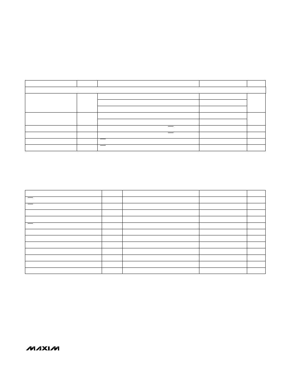
ELECTRICAL CHARACTERISTICS (continued)
(V+ = 5V, V- = -5V, DGND = AGND = IN LO = REF- = 0V, REF+ = 545mV, R
INT
= 602k
Ω
, C
INT
= 0.0047µF, C
REF
= 0.1µF,
f
CLK
= 32,768Hz, 60Hz mode, T
A
= T
MIN
to T
MAX
, unless otherwise noted.)
INTERFACE TIMING
(Test Circuit of Figure 1, Figure 2, V+ = 5V, V- = -5V, DGND = AGND = 0V, T
A
= +25°C, unless otherwise noted.) (Note 3)
Note 1:
±18-bit accuracy achieved by averaging multiple conversions.
Note 2:
Maximum deviation from best straight-line fit.
Note 3:
Guaranteed by design, not tested.
Note 4:
Difference in reading for equal positive and negative inputs near full scale.
DOUT, I
OUT
= -100µA
DOUT, I
OUT
= -1mA
CS, DIN, SCLK, and DOUT when three-stated
CS, DIN, SCLK, and DOUT when three-stated
Referred to DGND, 4.5V
≤
V+
≤
5.5V, CS, DIN, SCLK
EOC, P0–P3, I
OUT
= -100µA
DOUT, I
OUT
= 1.6mA
EOC, P0–P3, I
OUT
= 100µA
Referred to DGND, 4.5V
≤
V+
≤
5.5V, CS, DIN, SCLK
CONDITIONS
4.0
4.5
3.5
4.3
pF
5
C
IN
Input Capacitance
nA
±10
±500
I
IN
Input Current
V
0.8
V
IL
Input Low
V
4.0
4.7
V
OH
Output High
0.1
0.4
V
0.1
0.4
V
OL
Output Low
V
2.4
V
IH
Input High
UNITS
MIN
TYP
MAX
SYMBOL
PARAMETER
CONDITIONS
ns
500
t
1
CS Lead Time
µs
1
t
5
CS High Pulse Width
ns
300
t
4
S
CLK
Low Time
ns
400
t
3
S
CLK
High Time
ns
400
t
2
CS Lag Time
UNITS
MIN
TYP
MAX
SYMBOL
PARAMETER
See Figure 4
See Figure 3
ns
0
t
6
DIN to SCLK Setup Time
ns
320
t
10
DOUT Disable Time to Three-State
ns
60
t
9
Data Valid
ns
320
t
8
DOUT Access Time from Three-State
ns
200
t
7
DIN to SCLK Hold Time
ns
230
350
t
12
Delay to P0–P3 Low
ns
230
350
t
11
Delay to P0–P3 High
DIGITAL SECTION