Rainbow Electronics MAX132 User Manual
Page 2

MAX132
±18-Bit ADC with Serial Interface
2
_______________________________________________________________________________________
ABSOLUTE MAXIMUM RATINGS
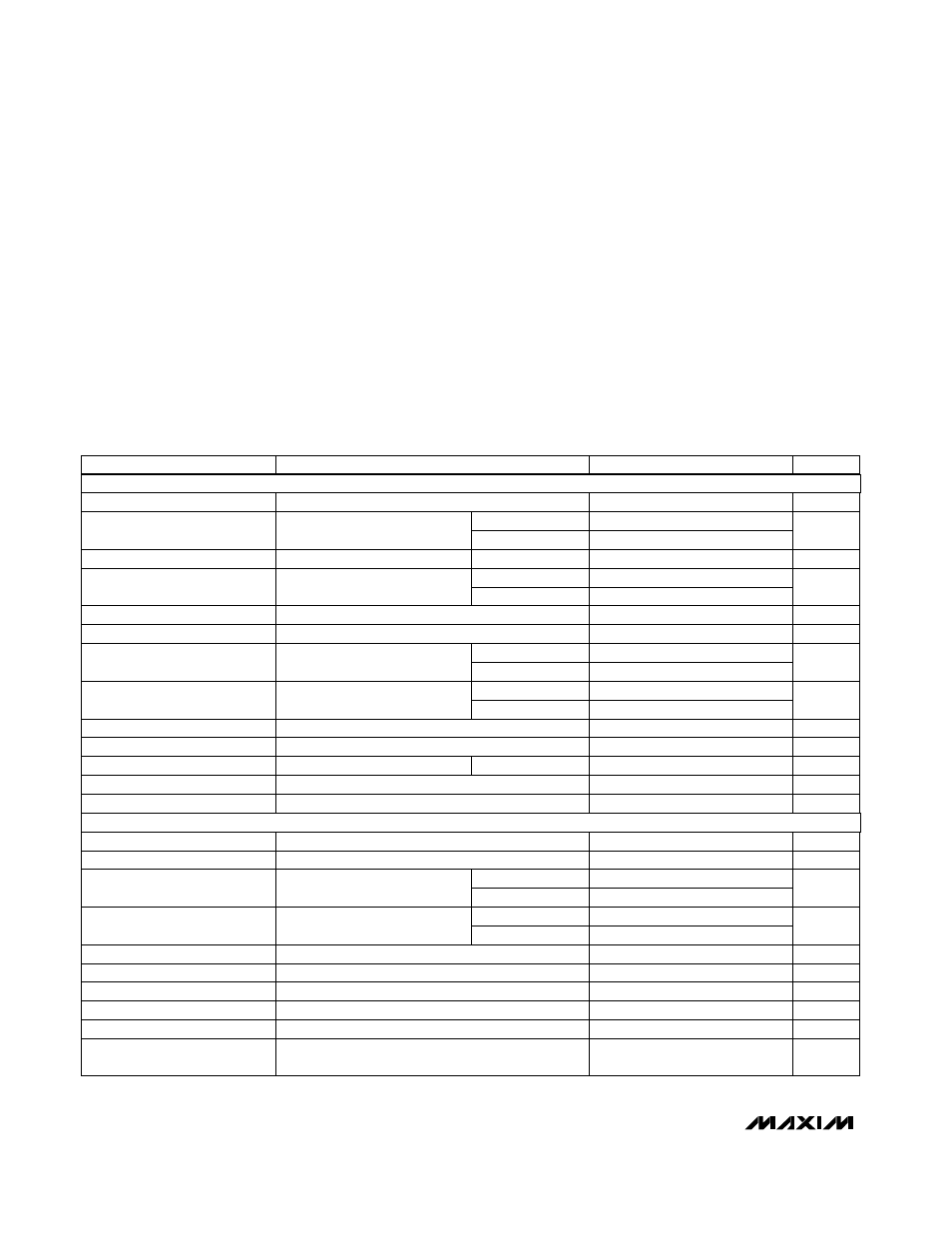
ELECTRICAL CHARACTERISTICS
(V+ = 5V, V- = -5V, DGND = AGND = IN LO = REF- = 0V, REF+ = 545mV, R
INT
= 602k
Ω
, C
INT
= 0.0047µF, C
REF
= 0.1µF,
f
CLK
= 32,768Hz, 60Hz mode, T
A
= T
MIN
to T
MAX
, unless otherwise noted.)
Stresses beyond those listed under “Absolute Maximum Ratings” may cause permanent damage to the device. These are stress ratings only, and functional
operation of the device at these or any other conditions beyond those indicated in the operational sections of the specifications is not implied. Exposure to
absolute maximum rating conditions for extended periods may affect device reliability.
Supply Voltage
V+ to DGND ..............................................-0.3V < V+ < +6.0V
V- to DGND ................................................+0.3V < V- < -9.0V
V+ to V- ............................................................................+15V
Analog Input Voltage (any input).....................................V+ to V-
Digital Input Voltage .....................(DGND - 0.3V) to (V+ + 0.3V)
Continuous Power Dissipation
Narrow Plastic DIP (derate 8.70mW/°C above +70°C)....478mW
Wide SO (derate 11.76mW/°C above +70°C)..............647mW
Narrow CERDIP (derate 12.50mW/°C above +70°C) ..688mW
Operating Temperature Ranges
MAX132C_ _ .......................................................0°C to +70°C
MAX132E_ _ ....................................................-40°C to +85°C
MAX132MRG .................................................-55°C to +125°C
Storage Temperature Range .............................-65°C to +160°C
Lead Temperature (soldering, 10sec) .............................+300°C
Bits
±18
Resolution
UNITS
MIN
TYP
MAX
PARAMETER
(Note 1)
CONDITIONS
V
IN
HI = 0V
% of FSR
±0.0168
0
±0.0076
Zero Error
f
CLK
= 32.768Hz
(Note 4)
ms
63
±0.032
Rollover Error
(Notes 2, 3)
% of FSR
0
±0.010
% of FSR
±0.0015
±0.006
Integral Nonlinearity
IN HI = IN LO
V
±3.0
Input Voltage Range
Common-Mode Range
(Note 3)
ppm/°C
±5
Scale Factor Temp. Coefficient
(Note 3)
ppm/°C
±0.15
±1.5
µV
15
RMS Noise
Zero-Reading Drift
mV
±512
Conversion Time
V
IN
HI = 400mV, V- = -5.0V,
4.5V
≤
V+
≤
5.5V
±0.003
±0.0168
% of FSR
±0.003
±0.0061
Positive Supply Rejection
Digital input = 0V or V+
Digital input = 0V or V+
µA
1
10
µA
-25
-60
Digital Ground Supply Current
Positive Sleep-Mode Current
Digital input = 0V or V+
Digital input = 0V or V+
µA
-35
-65
µA
60
125
Positive Supply Current
Negative Supply Current
Digital input = 0V or V+
µA
-1
-10
Negative Sleep-Mode Current
V
-5.5
-4.5
V
4.5
5.5
Positive Supply Voltage
Negative Supply Voltage
T
A
= +25°C
T
A
= T
MIN
to T
MAX
T
A
= +25°C
T
A
= +25°C
T
A
= T
MIN
to T
MAX
IN HI to IN LO, for specified accuracy
% of FSR
±0.25
±0.50
Common-Mode Rejection Ratio
IN HI = IN LO
±0.009
±0.032
V
CM
= ±500mV
V
CM
= ±3.0V
pA
±12
±250
Leakage Current
IN HI, IN LO
±2
±10
T
A
= +25°C
T
A
= T
MIN
to T
MAX
T
A
= +25°C
T
A
= T
MIN
to T
MAX
T
A
= T
MIN
to T
MAX
T
A
= +25°C
V
IN
HI = 400mV, V- = 5.0V,
-5.5V
≤
V-
≤
-4.5V
±0.003
±0.0168
% of FSR
±0.003
±0.0061
Negative Supply Rejection
Digital input = 0V or V+
µA
0
±2
Digital Ground Sleep-Mode
Current
T
A
= +25°C
% of FSR
±3.1
Read-Zero 50Hz/60Hz Range
ACCURACY
POWER REQUIREMENTS
