Rainbow Electronics MAX132 User Manual
Page 12
MAX132
±18-Bit ADC with Serial Interface
12
______________________________________________________________________________________
Command Input Register 1
User-Programmable Output Bits P0 to P3
Command input register 1 always has data bit D0 = 1.
Data bits D4 to D7 of command register 1 control the
states of the user-programmable output pins P0 to P3,
respectively (Table 2). These four outputs can be used
to control an external multiplexer, programmable gain
amplifier, or other devices.
Output Registers
Output data is the sum of system offset (read zero) plus
the results of the external input voltage measurement.
Register 0
Register 0 contains the low-byte (bits B3–B10) conver-
sion data. New data is available after EOC goes high.
Access register 0 by setting RS0 and RS1 to 0.
Register 1
Register 1 contains the high-byte (bits B11–B18) data.
Data is in a twos-complement format‚ where the polarity
bit is a 1 for negative polarity data. Access register 1
by setting control bits RS0 = 1 and RS1 = 0 when writ-
ing to the command input register.
Status Register
Bits B0–B2
The B0, B1, and B2 bits are located in the status regis-
ter. At the end of each conversion these bits are updat-
ed and read back from the status register. For full
18-bit resolution, use bits B0–B2. Average multiple
results to increase accuracy. The polarity bit informa-
tion is necessary to determine if the reading is not in
overrange (Tables 4 and 5).
Integrate Bit
The integrate (INT) bit is set to 1 at the beginning of the
integration phase and becomes 0 at the end. Poll INT
to determine the earliest time the input can be changed
without affecting the conversion.
End-of-Conversion Bit
The end-of-conversion (EOC) bit signals conversion sta-
tus. If EOC is 1, the conversion is complete and the ADC
waits in zero-integrate mode at time = 0000 for the next
start instruction. A conversion cycle has 2048 counts.
EOC becomes 1 at count 0000 and 0 at count 0001.
Collision Bit
The collision bit warns the microprocessor (µP) that the
register’s data was changed during the read cycle. A
collision occurs if the internal result latches on the falling
edge of CS, causing the collision bit to be set to 1 on the
rising edge of the next CS. This occurs because these
two pulses are asynchronous. Once the status register is
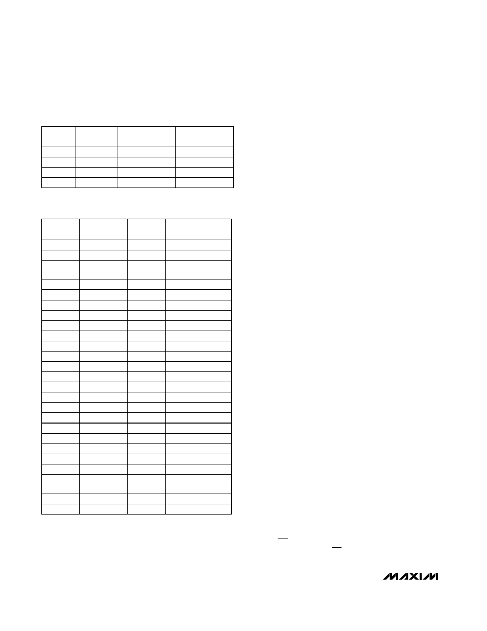
Table 4. Overrange Values for
Resolution Used
Table 5. Output Values for 16-Bit
Resolution (Offset Corrected)
Bits
Used
B18–B3
B18–B2
B18–B1
Resolution
Bits
±15
±16
±17
B18–B0
±18
Soft Overrange
Start Value
34,880
69,760
139,520
Hard Overrange
Maximum Value
43,805
87,610
175,220
279,040
350,440
Input
+640mV
+576mV
+545mV
Hexadecimal
Reading
+A000
+9000
+8840
Decimal
Counts
+40960*
+36864*
+34880*
+512mV
Comment
+8000
Positive Reference
Voltage
+32768
Positive Full Scale
+448mV
+384mV
+320mV
+7000
+6000
+5000
+28672
+24576
+20480
+256mV
+4000
+16384
+192mV
+128mV
+15µV
+3000
+2000
+0001
+12288
+8192
+1
0
+0000
0
-15µV
-64mV
-128mV
-FFFF
-F000
-E000
-1
-4096
-8192
-192mV
-D000
-12288
-256mV
-320mV
-384mV
-C000
-B000
-A000
-16384
-20480
-24576
-448mV
-9000
-28672
-512mV
-545mV
-576mV
-8000
-77C0
-7000
-32768
-34880*
-36864*
-640mV
Negative Full Scale
-6000
Negative Reference
Voltage
-40960*
+64mV
+1000
+4096
* Soft Overrange Operation
Note
: The MAX132 exhibits additional errors when operating
in the soft overrange area. Operation in this region is not
included in the specifications. The soft overrange values listed
in Table 5 do not include error correction.