Pin description – Rainbow Electronics MAX1421 User Manual
Page 9
MAX1421
12-Bit, 40Msps, +3.3V, Low-Power ADC
with Internal Reference
_______________________________________________________________________________________
9
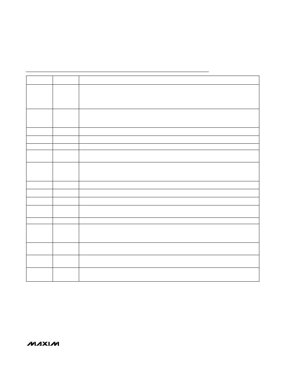
PIN
NAME
FUNCTION
1, 4, 5, 8,
9, 12, 13,
16, 19, 41,
48
AGND
Analog Ground. Connect all return paths for analog signals to AGND.
2, 3, 10,
11, 14, 15,
20, 42, 47
AV
DD
Analog Supply Voltage. For optimum performance bypass to the closest AGND with a parallel
combination of a 0.1
µF and a 1nF capacitor. Connect a single 10µF and 1µF capacitor combination
between AV
DD
and AGND.
6
INP
Positive Analog Signal Input
7
INN
Negative Analog Signal Input
17
CLK
Clock Frequency Input. Clock frequency input ranges from 100kHz to 40MHz.
18
CLK
Complementary Clock Frequency Input. This input is used for differential clock inputs. If the ADC is
driven with a single-ended clock, bypass
CLK with a 0.1
µF capacitor to AGND.
21, 31, 32,
DV
DD
Digital Supply Voltage. For optimum performance bypass, to the closest DGND with a parallel
combination of a 0.1
µF and a 1nF capacitor. Connect a single 10µF and 1µF capacitor combination
between DV
DD
and DGND.
22, 29, 30
DGND
Digital Ground
23–28
D0–D5
Digital Data Outputs. Data bits D0 through D5, where D0 represents the LSB.
33–38
D6–D11
Digital Data Outputs. D6 through D11, where D11 represents the MSB.
39
OE
Output Enable Input. A logic “1” on
OE places the outputs D0–D11 into a high-impedance state. A
logic “0” allows for the data bits to be read from the outputs.
40
PD
Shutdown Input. A logic “1” on PD places the ADC into shutdown mode.
43
REFIN
External Reference Input. Bypass to AGND with a capacitor combination of 0.22
µF in parallel with
1nF. REFIN can be biased externally to adjust reference levels and calibrate full-scale errors. To
disable the internal reference, connect REFIN to AGND.
44
REFP
P osi ti ve Refer ence I/O . Byp ass to AG N D w i th a cap aci tor com b i nati on of 0.22
µF i n p ar al l el w i th 1nF.
W i th the i nter nal r efer ence d i sab l ed ( RE FIN = AG N D ) , RE FP shoul d b e b i ased to V
C M L
+ V
D IF F
/ 2.
45
REFN
N eg ati ve Refer ence I/O . Byp ass to AG N D w i th a cap aci tor com b i nati on of 0.22
µF i n p ar al l el w i th 1nF.
W i th the i nter nal r efer ence d i sab l ed ( RE FIN = AG N D ) , RE FN shoul d b e b i ased to V
C M L
- V
D IF F
/ 2.
46
CML
Common-Mode Level Input. Bypass to AGND with a capacitor combination of 0.22
µF in parallel
with 1nF. With the internal reference disabled (REFIN = AGND).
Pin Description