Applications information, Ooe e – Rainbow Electronics MAX1421 User Manual
Page 12
MAX1421
12-Bit, 40Msps, +3.3V, Low-Power ADC
with Internal Reference
12
______________________________________________________________________________________
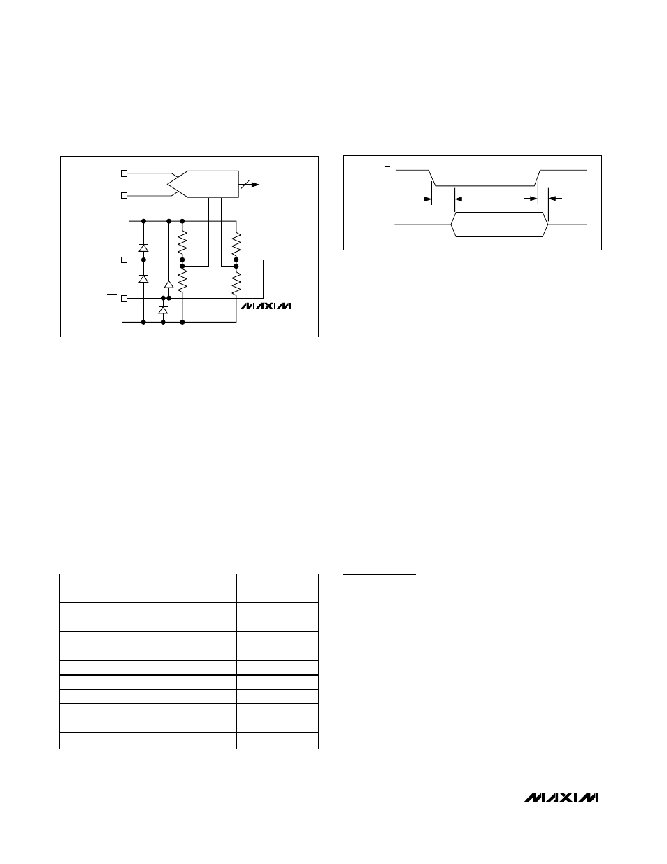
Figure 4 shows a simplified model of the clock input cir-
cuit. This circuit consists of two 10k
Ω resistors to bias
the common-mode level of each input. This circuit may
be used to AC-couple the system clock signal to the
MAX1421 clock input.
Output Enable (
O
OE
E
), Power-Down (PD), and
Output Data (D0–D11)
With OE high, the digital outputs enter a high-imped-
ance state. If OE is held low with PD high, the outputs
are latched at the last value prior to the power-down. All
data outputs, D0 (LSB) through D11 (MSB), are
TTL/CMOS-logic compatible. There is a seven clock-
cycle latency between any particular sample and its
valid output data. The output coding is in offset binary
format (Table 1).
The capacitive load on the digital outputs D0 through
D11 should be kept as low as possible (
≤10pF), to
avoid large digital currents that could feed back into
the analog portion of the MAX1421, thereby degrading
its dynamic performance. The use of digital buffers
(e.g., 74LVCH16244) on the digital outputs of the ADC
can further isolate the digital outputs from heavy capac-
itive loads. To further improve the dynamic perfor-
mance of the MAX1421, add small-series resistors of
100
Ω to the digital output paths, close to the ADC.
Figure 5 displays the timing relationship between out-
put enable and data output.
System Timing Requirements
Figure 6 depicts the relationship between the clock
input, analog input, and data output. The MAX1421
samples at the rising edge of CLK (falling edge of CLK)
and output data is valid seven clock cycles (latency)
later. Figure 6 also displays the relationship between
the input clock parameters and the valid output data.
Applications Information
Figure 7 depicts a typical application circuit containing
a single-ended to differential converter. The internal ref-
erence provides an AV
DD
/ 2 output voltage for level-
shifting purposes. The input is buffered and then split to
a voltage follower and inverter. A lowpass filter at the
input suppresses some of the wideband noise associat-
ed with high-speed op amps. Select the R
ISO
and C
IN
values to optimize the filter performance and to suit a
particular application. For the application in Figure 7, a
R
ISO
of 50
Ω is placed before the capacitive load to pre-
vent ringing and oscillation. The 22pF C
IN
capacitor
acts as a small bypassing capacitor.
Connecting C
IN
from INN to INP may further improve
dynamic performance.
D11–D0
10k
Ω
10k
Ω
10k
Ω
10k
Ω
A
VDD
ADC
CLK
CLK
INN
INP
AGND
MAX1421
Figure 4. Simplified Clock Input Circuit
OUTPUT
DATA D11–D0
OE
t
BD
t
BE
HIGH-Z
HIGH-Z
VALID DATA
Figure 5. Output Enable Timing
Table 1. MAX1421 Output Code for
Differential Inputs
DIFFERENTIAL
INPUT VOLTAGE*
DIFFERENTIAL
INPUT
OFFSET
BINARY
V
REF
× 2047/2048
+FULL SCALE -
1LSB
1111 1111 1111
V
REF
× 2046/2048
+FULL SCALE -
2LSB
1111 1111 1110
V
REF
× 1/2048
+ 1 LSB
1000 0000 0001
0
Bipolar Zero
1000 0000 0000
-V
REF
× 1/2048
- 1 LSB
0111 1111 1111
-V
REF
× 2046/2048
-FULL SCALE +
1 LSB
0000 0000 0001
-V
REF
× 2047/2048
-FULL SCALE
0000 0000 0000
* V
REF
= V
REFP
- V
REFN