Grounding, bypassing, and board layout – Rainbow Electronics MAX1421 User Manual
Page 13

MAX1421
12-Bit, 40Msps, +3.3V, Low-Power ADC
with Internal Reference
______________________________________________________________________________________
13
Using Transformer Coupling
An RF transformer (Figure 8) provides an excellent solu-
tion to convert a single-ended signal to a fully differen-
tial signal, required by the MAX1421 for optimum
performance. Connecting the center tap of the trans-
former to CML provides an AV
DD
/ 2 DC level shift to
the input. Although a 1:1 transformer is shown, a 1:2 or
1:4 step-up transformer may be selected to reduce the
drive requirements.
In general, the MAX1421 provides better SFDR and
THD with fully differential input signals over single-
ended input signals, especially for very high input fre-
quencies. In differential input mode, even-order
harmonics are suppressed and each of the inputs
requires only half the signal swing compared to single-
ended mode.
Single-Ended AC-Coupled Input Signal
Figure 9 shows an AC-coupled, single-ended applica-
tion, using a MAX4108 op amp. This configuration pro-
vides high-speed, high-bandwidth, low noise, and low
distortion to maintain the integrity of the input signal.
Grounding, Bypassing, and
Board Layout
The MAX1421 requires high-speed board layout design
techniques. Locate all bypass capacitors as close to
the device as possible, preferably on the same side of
the board as the ADC, using surface-mount devices for
minimum inductance. Bypass REFP, REFN, REFIN, and
CML with a parallel network of 0.22µF capacitors and
1nF to AGND. AV
DD
should be bypassed with a similar
network of a 10µF bipolar capacitor in parallel with two
ceramic capacitors of 1nF and 0.1µF. Follow the same
rules to bypass the digital supply DV
DD
to DGND.
Multilayer boards with separate ground and power
planes produce the highest level of signal integrity.
Consider the use of a split ground plane arrangement
to match the physical location of the analog ground
(AGND) and the digital output driver ground (DGND) on
the ADCs package. The two ground planes should be
joined at a single point so that the noisy digital ground
currents do not interfere with the analog ground plane.
Alternatively, all ground pins could share the same
ground plane, if the ground plane is sufficiently isolated
from any noisy, digital systems ground plane (e.g.,
downstream output buffer, DSP ground plane). Route
high-speed digital signal traces away from sensitive
analog traces and remove digital ground and power
planes from underneath digital outputs. Keep all signal
lines short and free of 90 degree turns.
Static Parameter Definitions
Integral Nonlinearity (INL)
Integral nonlinearity is the deviation of the values on an
actual transfer function from a straight line. This straight-
line can be either a best straight-line fit or a line drawn
between the endpoints of the transfer function, once off-
set and gain errors have been nullified. The static lin-
earity parameters for the MAX1421 are measured using
the best straight-line fit method.
Differential Nonlinearity (DNL)
Differential nonlinearity is the difference between an
actual step-width and the ideal value of 1LSB. A DNL
N - 7
N
N - 6
N + 1
N - 5
N + 2
N - 4
N + 3
N - 3
N + 4
N - 2
N + 5
N - 1
N
N + 6
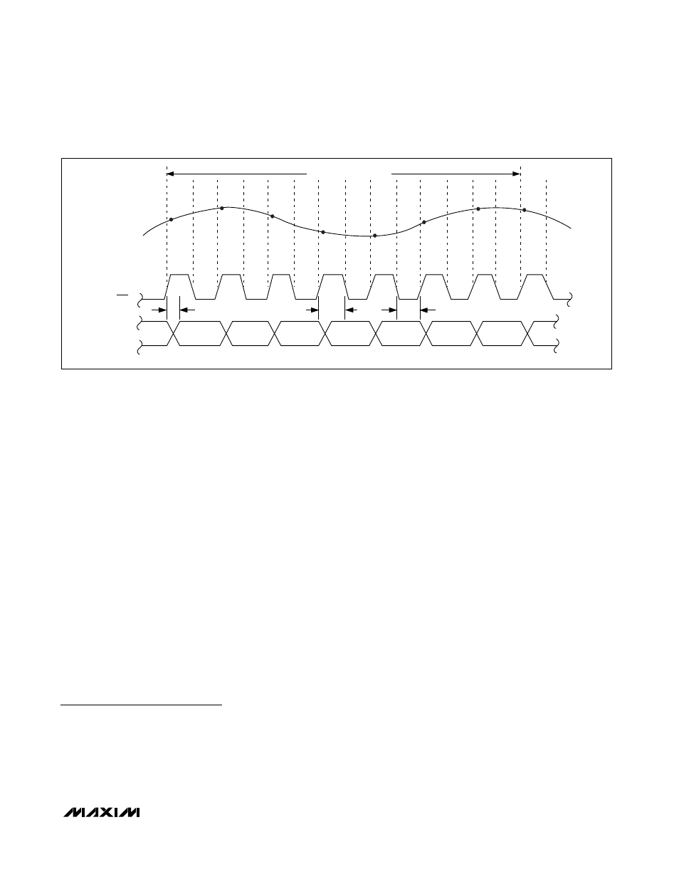
7 CLOCK-CYCLE LATENCY
ANALOG INPUT
DATA OUTPUT
t
DO
t
CH
t
CL
CLK
CLK
Figure 6. System and Output Timing Diagram
