Ccl lk k – Rainbow Electronics MAX1421 User Manual
Page 11
MAX1421
12-Bit, 40Msps, +3.3V, Low-Power ADC
with Internal Reference
______________________________________________________________________________________
11
The MAX1421 provides three modes of reference oper-
ation:
•
Internal reference mode
•
Buffered external reference mode
•
Unbuffered external reference mode
In internal reference mode, the on-chip +2.048V
bandgap reference is active and REFIN, REFP, CML,
and REFN are left floating. For stability purposes,
bypass REFIN, REFP, REFN, and CML with a capacitor
network of 0.22µF, in parallel with a 1nF capacitor to
AGND.
In buffered external reference mode, the reference volt-
age levels can be adjusted externally by applying a
stable and accurate voltage at REFIN.
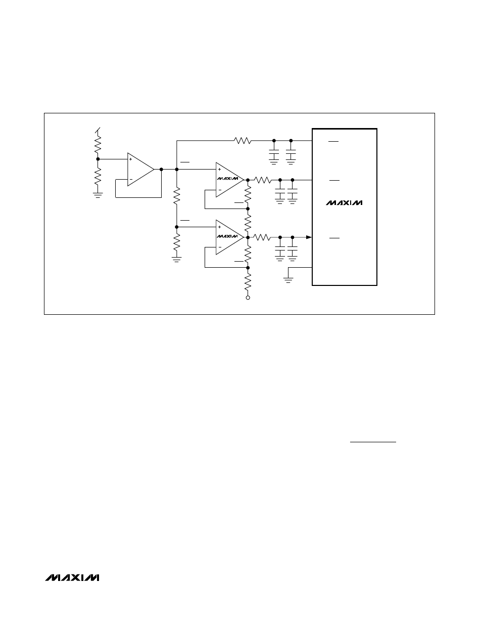
In unbuffered external reference mode, REFIN is con-
nected to AGND, which deactivates the on-chip buffers
of REFP, CML, and REFN. With their buffers shut down,
these nodes become high impedance and can be dri-
ven by external reference sources, as shown in Figure 3.
Clock Inputs (CLK,
C
CL
LK
K
)
The MAX1421’s CLK and CLK inputs accept both sin-
gle-ended and differential input operation, and accept
CMOS-compatible clock signals. If CLK is driven with a
single-ended clock signal, bypass CLK with a 0.1µF
capacitor to AGND. Since the interstage conversion of
the device depends on the repeatability of the rising
and falling edges of the external clock, use a clock with
low jitter and fast rise and fall times (<2ns). In particu-
lar, sampling occurs on the rising edge of the clock sig-
nal, requiring this edge to have the lowest possible
jitter. Any significant aperture jitter limits the SNR per-
formance of the ADC according to the following rela-
tionship:
where f
IN
represents the analog input frequency and
t
AJ
is the aperture jitter.
Clock jitter is especially critical for high input frequency
applications. The clock input should always be consid-
ered as an analog input and routed away from any ana-
log or digital signal lines.
The MAX1421 clock input operates with a voltage
threshold set to AV
DD
/ 2. Clock inputs must meet the
specifications for high and low periods, as stated in the
Electrical Characteristics.
S
1
2
t
dB
IN
AJ
NR
=
Ч
Ч
Ч
20
10
log
π ƒ
MAX1421
REFIN
REFN
R
50
Ω
R
R
R
R
+1V
R
50
Ω
50
Ω
R
R
AV
DD
CML
1nF
0.22
µF
1nF
0.22
µF
1nF
0.22
µF
AGND
AV
DD
2
AV
DD
4
MAX4284
MAX4284
( )
REFP
+ 1V
( )
AV
DD
2
+ 1V
( )
AV
DD
2
AV
DD
2
AV
DD
4
AV
DD
2
Figure 3. Unbuffered External Reference Drive—Internal Reference Disabled