Pmics with dynamic core for pdas and smart phones, Electrical characteristics (continued) – Rainbow Electronics MAX1587A User Manual
Page 4
MAX1586A/MAX1586B/MAX1587A
High-Efficiency, Low-I
Q
PMICs with
Dynamic Core for PDAs and Smart Phones
4
_______________________________________________________________________________________
PARAMETER
CONDITIONS
MIN
TYP
MAX
UNITS
I
LX3
= -180mA
0.225
0.375
P-Channel On-Resistance
I
LX2
= -180mA, V
PV3
= 2.6V
0.26
0.425
Ω
I
LX3
= 180mA
0.15
0.25
N-Channel On-Resistance
I
LX3
= 180mA, V
PV3
= 2.6V
0.17
0.275
Ω
Current-Sense Transresistance
1.25
V/A
P-Channel Current-Limit Threshold
-0.60
-0.7
-0.85
A
PWM Skip-Mode Transition Load
Current
Decreasing load current (Note 2)
30
mA
OUT3 Maximum Output Current
2.6V
≤
V
PV3_
≤
5.5V (Note 3)
0.5
A
LX3 Leakage Current
V
PV3_
= 5.5V, LX3 = GND or PV2, V
ON3
= 0V
-10
+0.1
+10
µA
LDOS V4, V5, V6, V1 SLEEP, V2 SLEEP, AND V7 OUTPUT
V4, V5, V6, V1 SLEEP, V2 SLEEP
Output Current
35
mA
V7 Output Current
30
mA
REG4 Output Voltage
Load = 0.1 to 35mA
1.261
1.3
1.339
V
REG4 Noise
With 1µF C
OUT
and 0.01µF C
BYP
15
µVRMS
REG5 Output Voltage
Load = 0.1mA to 35mA
1.067
1.1
1.133
V
IN45, IN6 Input Voltage Range
2.4
5.5
V
0V setti ng ( ei ther ON 6 l ow or ser i al p r og r am m ed )
0
1.8V setting, load = 0.1mA to 35mA
1.746
1.8
1.854
2.5V setting, load = 0.1mA to 35mA
2.425
2.5
2.575
REG6 Output Voltage (POR Default
to 0V, Set by Serial Input)
MAX1586
3.0V setting, load = 0.1mA to 35mA
2.91
3.0
3.09
V
V1 on and in regulation
V
V1
V7 Output Voltage
V1 off
V
BKBT
V
V1 and V2 SLEEP Output Voltage
Accuracy
Set to same output voltage as REG1 and REG2
-3.0
+3.0
%
V1 and V2 SLEEP Dropout Voltage
LOAD = 20mA
75
150
mV
V6 Dropout Voltage
M AX 1586 3V m od e, l oad = 30m A, 2.5V m od e, l oad = 30m A
110
200
mV
V7 Switch Voltage Drop
LOAD = 20mA, V
BKBT
= V
V1
= 3.0V
100
200
mV
V4, V5, V6 Output Current Limit
40
90
mA
BKBT Leakage
1
µA
OSCILLATOR
PWM Switching Frequency
0.93
1
1.07
MHz
SUPERVISORY/MANAGEMENT FUNCTIONS
Rising
92
94.75
97
POK Trip Threshold (Note 4)
Falling
88.5
90.5
92.5
%
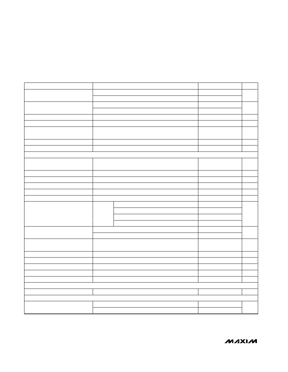
ELECTRICAL CHARACTERISTICS (continued)
(V
IN
= 3.6V, V
BKBT
= 3.0V, V
LBI
= 1.1V, V
DBI
= 1.35V, circuit of Figure 5,
T
A
= 0°C to +85°C, unless otherwise noted. Typical values
are at T
A
= +25
°C.)