Pmics with dynamic core for pdas and smart phones, Pin description – Rainbow Electronics MAX1587A User Manual
Page 14
MAX1586A/MAX1586B/MAX1587A
High-Efficiency, Low-I
Q
PMICs with
Dynamic Core for PDAs and Smart Phones
14
______________________________________________________________________________________
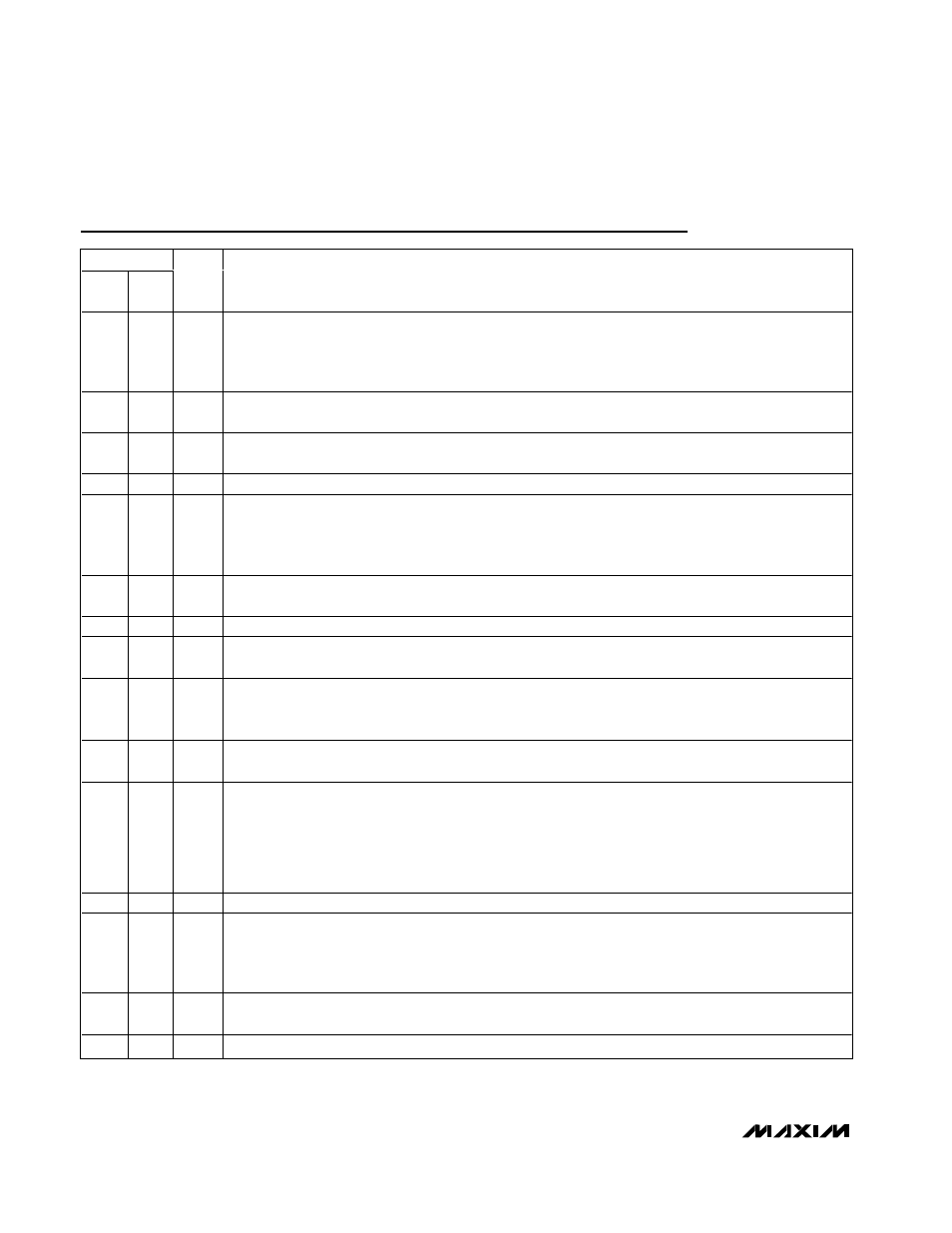
Pin Description
PIN
MAX
1586
MAX
1587
NAME
FUNCTION
1
—
LBI
Dual-Mode™, Low-Battery Input. Connect to IN to set the low-battery threshold to 3.6V (no resistors
needed). Connect LBI to a resistor-divider for an adjustable LBI threshold. When IN is below the set
threshold, LBO output switches low. LBO is deactivated and forced low when IN is below the dead-battery
(DBI) threshold and when all REGs are disabled.
2
40
CC1
REG1 Compensation Node. Connect a series resistor and capacitor from CC1 to GND to compensate the
regulation loop. See the Compensation and Stability section.
3
1
FB1
REG1 Feedback Input. Connect to IN to set V1 to 3.0V or connect FB1 to GND to set V1 to 3.3V. Connect
FB1 to external feedback resistors for other output voltages.
4
2
BKBT
Input Connection for Backup Battery. This input can also accept the output of an external boost converter.
5
3
V7
Also known as VCC_BATT. V7 is always active if main or backup power is present. It is the first regulator
that powers up. V7 has two states:
1) V7 tracks V1 if ON1 is high and V1 is in regulation.
2) V7 tracks V
BKBT
when ON1 is low or V1 is out of regulation.
6
4
V1
REG1 Voltage-Sense Input. Connect directly to the REG1 output voltage. The output voltage is set by FB1
to either 3.0V, 3.3V, or adjustable with resistors.
7
5
SLPIN
Inp ut to V 1 and V 2 S l eep Reg ul ator s. The i np ut to the stand b y r eg ul ator s at V 1 and V 2. C onnect S LP IN to IN .
8
6
V2
REG2 Voltage-Sense Input. Connect directly to the REG2 output voltage. The output voltage is set by FB2
to either 1.8V/2.5V (MAX1586A, MAX1587A), 3.3V/2.5V (MAX1586B), or adjustable with resistors.
9
7
FB2
REG2 Feedback Input. Connect to GND to set V2 to 2.5V on all devices. Connect FB2 to IN to set V2 to
1.8V on the MAX1586A and MAX1587A. Connect FB2 to IN to set V2 to 3.3V on the MAX1586B. Connect
FB2 to external feedback resistors for other voltages.
10
8
CC2
REG2 Compensation Node. Connect a series resistor and capacitor from CC2 to GND to compensate the
regulation loop. See the Compensation and Stability section.
11
9
POK
Power-OK Output. Open-drain output that is low when any of the V1–V6 outputs are below their regulation
threshold. When all activated outputs are in regulation, POK is high impedance. POK maintains a valid low
output with V7 as low as 1V. POK does not flag an out-of-regulation condition while REG3 is transitioning
between voltages set by serial programming. POK also does not flag for any REG channel that has been
turned off; however, if all REG channels are off (V1–V6), then POK is forced low. If IN < UVLO, then POK is
low. POK is expected to connect to nVCC_FAULT.
12
10
SCL
Serial Clock Input
13
11
SDA
Serial Data Input. Data is read on the rising edge of SCL. Serial data programs the REG3 (core) and REG6
(VCC_USIM) voltage. REG3 and REG6 can be programmed even when off, but at least one of the ON_ pins
must be logic-high to activate the serial interface. On power-up, REG3 defaults to 1.3V and REG6 defaults
to 0V.
14
12
PWM3
Force V3 to PWM at All Loads. Connect PWM3 to GND for normal operation (skip mode at light loads). Drive
or connect high for forced-PWM operation at all loads for V3 only.
15
—
LBO
Low-Battery Output. Open-drain output that goes low when IN is below the threshold set by LBI.
Dual Mode is a trademark of Maxim Integrated Products, Inc.