Pmics with dynamic core for pdas and smart phones, Chip information, Pin configurations – Rainbow Electronics MAX1587A User Manual
Page 28: Pc board layout and routing, Increasing v3 (vcc_core) voltage range
MAX1586A/MAX1586B/MAX1587A
High-Efficiency, Low-I
Q
PMICs with
Dynamic Core for PDAs and Smart Phones
28
______________________________________________________________________________________
active. In addition to biasing V7, the rechargeable bat-
tery may be required to also power other supplies.
Rechargeable NiMH Backup Battery
In some systems, a NiMH battery may be desired for
backup. Usually this requires multiple cells because
the typical NiMH cell voltage is only 1.2V. By adding a
small DC-DC converter (MAX1724), the low-battery
voltage is boosted to 3V to bias BKBT (Figure 8). The
DC-DC converter’s low operating current (1.5µA typ)
allows it to remain on constantly so the 3V BKBT bias is
always present. A resistor and diode trickle charge the
NiMH cell when the main power is present.
PC Board Layout and Routing
Good PC board layout is important to achieve optimal
performance. Conductors carrying discontinuous cur-
rents and any high-current path should be made as
short and wide as possible. A separate low-noise
ground plane containing the reference and signal
grounds should connect to the power-ground plane at
only one point to minimize the effects of power-ground
currents. Typically, the ground planes are best joined
right at the IC.
Keep the voltage feedback network very close to the
IC, preferably within 0.2in (5mm) of the FB_ pin. Nodes
with high dV/dt (switching nodes) should be kept as
small as possible and should be routed away from
high-impedance nodes such as FB_. Refer to the
MAX1586 or MAX1587 evaluation kit data sheets for a
full PC board example.
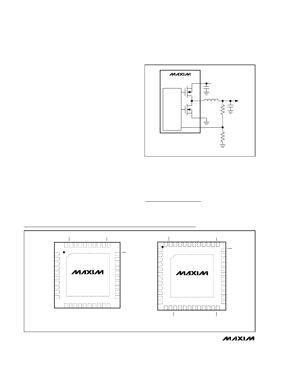
Increasing V3 (VCC_CORE) Voltage Range
The programmable V3 output voltage range can be
increased by adding two resistors as shown in Figure 9.
Chip Information
TRANSISTOR COUNT: 13,958
PROCESS: BiCMOS
TOP VIEW
RSO
SRAD
LX3
PG3
V4
ON45
ON2
V5
IN45
PV3
V7
V1
SLPIN
V2
FB2
CC2
POK
SCL
BKBT
FB1
1
2
3
4
5
6
7
8
9
10
11
12
13
14
15
16
17
18
19
20
40
39
38
37
36
35
34
33
32
31
30
29
28
27
26
25
24
23
22
21
PG2
IN
RAMP
REF
BYP
LX2
PV2
PWM3
SDA
SLP
PV1
LX1
PG1
ON1
ON3
FB3
CC3
MR
CC1
THIN QFN
6mm
×
6mm
MAX1587AETL
GND
RSO
SRAD
LX3
PG3
V4
ON4
ON2
ON5
ON3
V5
IN45
PV3
V7
V1
SLPIN
V2
FB2
CC2
CC1
POK
SCL
BKBT
FB1
LB1
PG2
IN
RAMP
REF
BYP
LX2
PV2
LBO
PWM3
SDA
SLP
PV1
LX1
PG1
IN6
V6
ON6
ON1
FB3
CC3
MR
DBI
THIN QFN
7mm
×
7mm
MAX1586AETM
MAX1586BETM
GND
DBO
1
2
3
4
5
6
7
8
9
10
11
12
36
35
34
33
32
31
30
29
28
27
26
25
48
47
46
45
44
43
42
41
40
39
38
37
13
14
15
16
17
18
19
20
21
22
23
24
Pin Configurations
PV3
STEP-DOWN
PWM
REG3
R24 VALUES:
R24 = 3.32kΩ, V3: 0.73V TO 1.55V, 26mV/STEP
R24 = 5.11kΩ, V3: 0.75V TO 1.60V, 27mV/STEP
R24 = 7.5kΩ, V3: 0.78V TO 1.65V, 28mV/STEP
LX3
PG3
FB3
V3
VCC_CORE
TO BATT
R25
100kΩ
R24
MAX1586
MAX1587
Figure 9. Adding R24 and R25 to Increase Core Voltage
Programming Range