Pmics with dynamic core for pdas and smart phones, Table 4. compensation parameters, Table 5. typical compensation values – Rainbow Electronics MAX1587A User Manual
Page 25
MAX1586A/MAX1586B/MAX1587A
High-Efficiency, Low-I
Q
PMICs with
Dynamic Core for PDAs and Smart Phones
______________________________________________________________________________________
25
must also have low impedance at the switching fre-
quency. Ceramic, polymer, and tantalum capacitors
are suitable, with ceramic exhibiting the lowest ESR
and lowest high-frequency impedance.
Output ripple with a ceramic output capacitor is
approximately:
V
RIPPLE
= I
L(PEAK)
[1 / (2π x f
OSC
x C
OUT
)]
If the capacitor has significant ESR, the output ripple
component due to capacitor ESR is:
V
RIPPLE(ESR)
= I
L(PEAK)
x ESR
Output capacitor specifics are also discussed in the
Compensation and Stability section.
Compensation and Stability
The relevant characteristics for REG1, REG2, and
REG3 compensation are:
1) Transconductance (from FB_ to CC_), gm
EA
2) Current-sense amplifier transresistance, R
CS
3) Feedback regulation voltage, V
FB
(1.25V)
4) Step-down output voltage, V
OUT
, in V
5) Output load equivalent resistance, R
LOAD
= V
OUT
/
I
LOAD
The key steps for step-down compensation are:
1) Set the compensation RC zero to cancel the R
LOAD
C
OUT
pole.
2) Set the loop crossover at or below approximately
1/10th the switching frequency.
For example, with V
IN(MAX)
= 5V, V
OUT
= 2.5V for
REG2, and I
OUT
= 800mA, then R
LOAD
= 3.125Ω. For
REG2, R
CS
= 0.75V/A and gm
EA
= 87µS.
Choose the crossover frequency, f
C
≤ f
OSC
/ 10.
Choose 100kHz. Then calculate the value of the com-
pensation capacitor, C
C
:
C
C
= (V
FB
/ V
OUT
) x (R
LOAD
/ R
CS
) x (gm / (2π x f
C
))
= (1.25 / 2.5) x (3.125 / 0.75) x (87 x 10
-6
/ (6.28
x 100,000)) = 289pF
Choose 330pF, the next highest standard value.
Now select the compensation resistor, R
C
, so transient-
droop requirements are met. As an example, if 3% tran-
sient droop is allowed for the desired load step, the
input to the error amplifier moves 0.03 x 1.25V, or
37.5mV. The error-amplifier output drives 37.5mV x
gm
EA
, or I
EAO
= 37.5mV x 87µS = 3.26µA across R
C
to
provide transient gain. Find the value of R
C
that allows
the required load-step swing from:
R
C
= R
CS
x I
IND(PK)
/ I
EAO
where I
IND(PK)
is the peak inductor current. In a step-
down DC-DC converter, if L
IDEAL
is used, output cur-
rent relates to inductor current by:
I
IND(PK)
= 1.25 x I
OUT
So for an 800mA output load step with V
IN
= 3.6V and
V
OUT
= 2.5V:
R
C
= R
CS
x I
IND(PK)
/ I
EAO
= (0.75V/A) x
(1.25 x 0.8A) / 3.26µA = 230kΩ
We choose 240kΩ. Note that the inductor does not limit
the response in this case since it can ramp at (V
IN
-
V
OUT
) / L, or (3.6 - 2.5) / 3.3µH = 242mA/µs.
The output filter capacitor is then selected so that the
C
OUT
R
LOAD
pole cancels the R
C
C
C
zero:
C
OUT
x R
LOAD
= R
C
x C
C
For the example:
R
LOAD
= V
OUT
x I
LOAD
= 2.5V / 0.8A =
3.125Ω
C
OUT
= R
C
x C
C
/ R
LOAD
= 240kΩ x 330pF /
3.125Ω = 25µF
We choose 22µF.
Recalculate R
C
using the selected C
OUT
.
R
C
= C
OUT
x R
LOAD
/ C
C
= 208kΩ
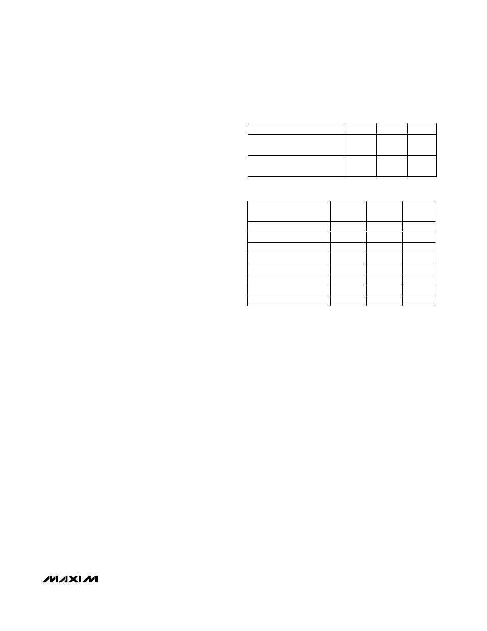
PARAMETER
REG1
REG2
REG3
Error-Amplifier
Transconductance, gmEA
87µS
87µS
68µS
Current-Sense Amp
Transresistance, R
CS
0.5V/A
0.75V/A
1.25V/A
Table 4. Compensation Parameters
COMPONENT OR
PARAMETER
REG1
REG2
REG3
V
OUT
3.3V
2.5V
1.3V
Output Current
1300mA
900mA
500mA
Inductor
3.3µH
6.8µH
10µH
Load-Step Droop
3%
3%
3%
Loop Crossover Freq (fC)
100kHz
100kHz
100kHz
C
C
330pF
270pF
330pF
R
C
240k
Ω
240k
Ω
240k
Ω
C
OUT
22µF
22µF
22µF
Table 5. Typical Compensation Values