Pmics with dynamic core for pdas and smart phones – Rainbow Electronics MAX1587A User Manual
Page 21
MAX1586A/MAX1586B/MAX1587A
High-Efficiency, Low-I
Q
PMICs with
Dynamic Core for PDAs and Smart Phones
______________________________________________________________________________________
21
also be used for only one of DBI or LBI. The other
threshold can then be factory set by connecting the
appropriate input to IN.
If BKBT is not powered, DBO does not function and is
high impedance. DBO is expected to connect to
nBATT_FAULT on Intel CPUs. If BKBT is not powered,
LBO does not function and is high impedance.
Power-OK Output (POK)
POK is an open-drain output that goes low when any
activated regulator (V1–V6) is below its regulation
threshold. POK does not monitor V7. When all active
output voltages are within 10% of regulation, POK is
high impedance. POK does not flag an out-of-regula-
tion condition while V3 is transitioning between voltages
set by serial programming or when any regulator chan-
nel has been turned off. POK momentarily goes low
when any regulator is turned on, but returns high when
that regulator reaches regulation. When all regulators
(V1–V6) are off, POK is forced low. If the input voltage
is below the UVLO threshold, POK is held low and
maintains a valid low output with IN as low as 1V. If
BKBT is not powered, POK does not function and is
high impedance.
Connection to Processor
and Power Sequencing
Typical processor connections have only power-control
pins, typically labeled PWR_EN and SYS_EN. The
MAX1586/MAX1587 provide numerous on/off control
pins for maximum flexibility. In a typical application,
many of these pins are connected together. ON1, ON2,
and ON6 typically connect to SYS_EN. ON3, ON4, and
ON5 typically connect to PWR_EN. V7 remains on as long
as the main or backup power is connected. Sequencing
is not performed internally on the MAX1586/MAX1587;
however, all ON_ inputs have hysteresis and can connect
to RC networks to set sequencing. For typical connec-
tions to Intel CPUs, no external sequencing is required.
Backup-Battery Input
The backup-battery input (BKBT) provides backup
power for V7 when V1 is disabled. Normally, a primary
or rechargeable backup battery is connected to this
pin. If a backup battery is not used, then BKBT should
connect to IN through a diode or external regulator. See
the Backup-Battery Configurations section for informa-
tion on how to use BKBT and V7.
Serial Interface
An I
2
C-compatible, two-wire serial interface controls
REG3 on the MAX1587, and REG3 and REG6 on the
MAX1586. The serial interface operates when IN exceeds
the 2.40V UVLO threshold and at least one of ON1–ON6
is asserted. The serial interface is shut down to minimize
off-current drain when no regulators are enabled.
The serial interface consists of a serial data line (SDA)
and a serial clock line (SCL). Standard I
2
C-compatible
write-byte commands are used. Figure 4 shows a tim-
ing diagram for the I
2
C protocol. The MAX1586/
MAX1587 are slave-only devices, relying upon a master
to generate a clock signal. The master (typically a
microprocessor) initiates data transfer on the bus and
generates SCL to permit data transfer. A master device
communicates to the MAX1586/MAX1587 by transmit-
ting the proper address followed by the 8-bit data code
(Table 2). Each transmit sequence is framed by a
START (A) condition and a STOP (L) condition. Each
word transmitted over the bus is 8 bits long and is
always followed by an acknowledge clock pulse.
Table 2 shows the serial data codes used to program
V3 and V6. The default power-up voltage for V3 is 1.3V
and for V6 is 0V.
MAX1586
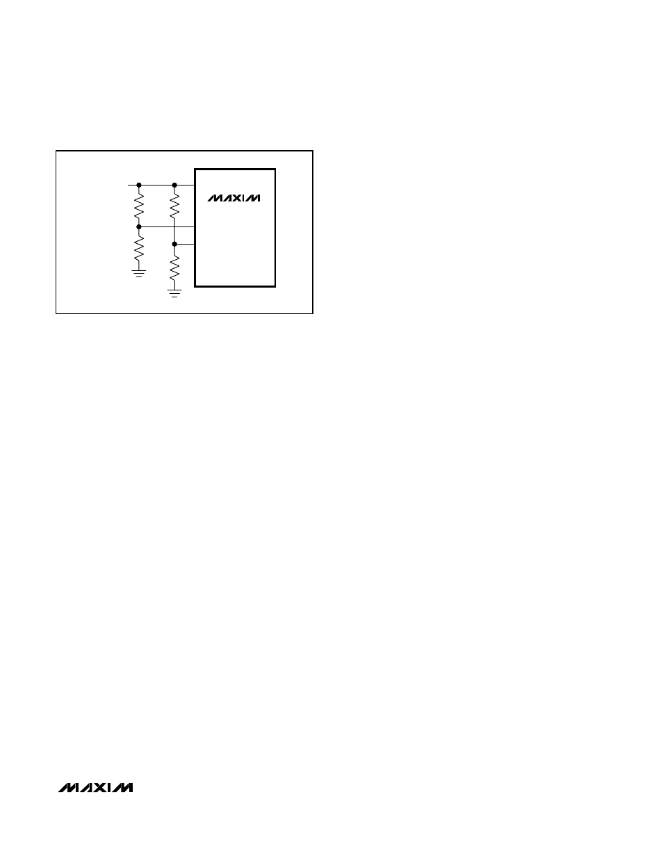
MAIN BATTERY
R6
500kΩ
R7
200kΩ
IN
DBI (1.232V THRESHOLD)
LBI (1.00V THRESHOLD)
R5
200kΩ
R4
334kΩ
Figure 3. Setting the Low-Battery and Dead-Battery Thresholds
with Separate Resistor-Dividers. The values shown set a DBI
threshold of 3.3V and an LBI threshold of 3.5V (no resistors are
needed for factory-preset thresholds).