Applications information, Parameter definitions – Rainbow Electronics MAX1127 User Manual
Page 22
MAX1127
Quad, 12-Bit, 65Msps, 1.8V ADC with
Serial LVDS Outputs
22
______________________________________________________________________________________
Global Power-Down (PDALL)
PDALL controls the power-down mode of all channels
and the internal reference circuitry. Drive PDALL high
to enable global power-down. In global power-down
mode, the output impedance of all the LVDS/SLVS out-
puts is approximately 378Ω, if DT is low. The output
impedance of the differential LVDS/SLVS outputs is
100Ω when DT is high. See the Electrical
Characteristics table for typical supply currents with
global power-down. The following list shows the state of
the analog inputs and digital outputs in global power-
down mode:
• IN_P, IN_N analog inputs are disconnected from the
internal input amplifier.
• REFIO has > 1MΩ resistance to GND.
• OUT_P, OUT_N, CLKOUTP, CLKOUTN, FRAMEP,
and FRAMEN have approximately 378Ω between the
output pairs when DT is low. When DT is high, the dif-
ferential output pairs have 100Ω between each pair.
When operating from the internal reference, the wake-
up time from global power-down is typically 132µs.
When using an external reference, the wake-up time is
dependent on the external reference drivers.
Applications Information
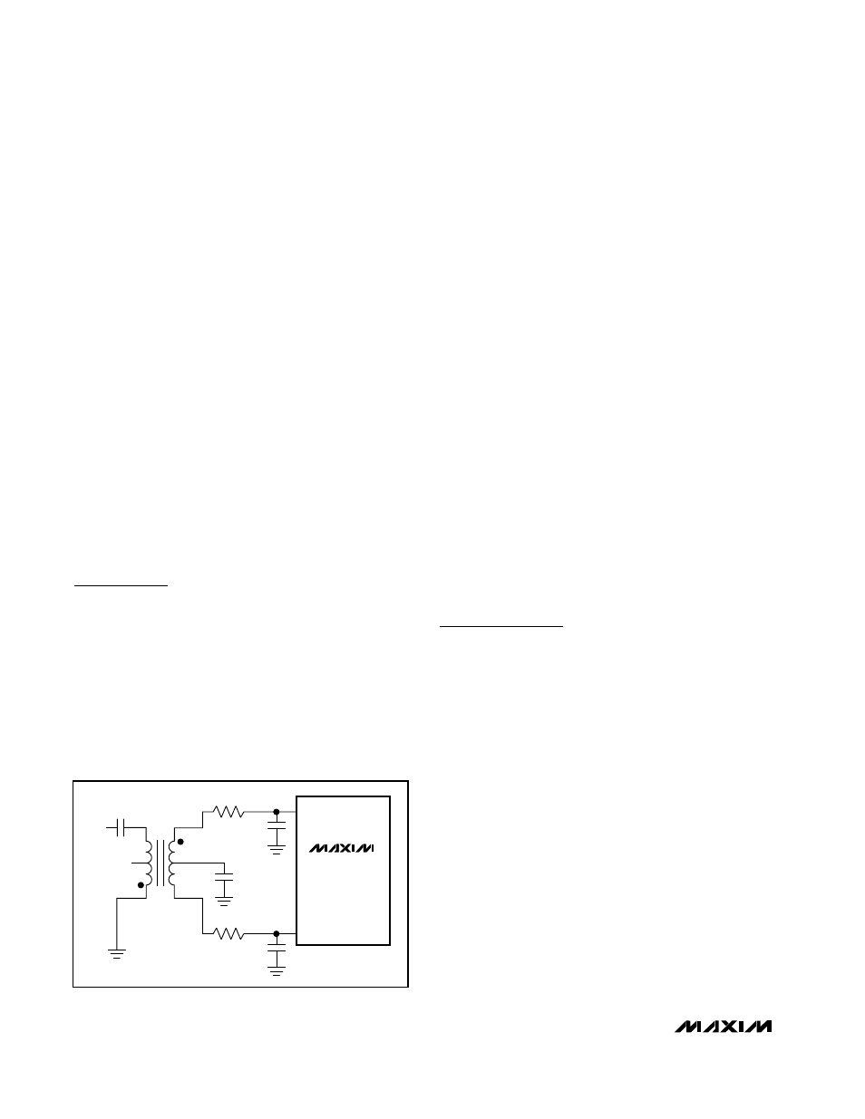
Using Transformer Coupling
An RF transformer (Figure 9) provides an excellent
solution to convert a single-ended input source signal
to a fully differential signal, required by the MAX1127
for optimum performance. The MAX1127 input com-
mon-mode voltage is internally biased to 0.6V (typ) with
f
CLK
= 65MHz. Although a 1:1 transformer is shown, a
step-up transformer can be selected to reduce the
drive requirements. A reduced signal swing from the
input driver, such as an op amp, can also improve the
overall distortion.
Grounding, Bypassing, and Board Layout
The MAX1127 requires high-speed board layout design
techniques. Refer to the MAX1127 EV kit data sheet for
a board layout reference. Locate all bypass capacitors
as close to the device as possible, preferably on the
same side as the ADC, using surface-mount devices
for minimum inductance. Bypass AV
DD
to GND with a
0.1µF ceramic capacitor in parallel with a ≥2.2µF
ceramic capacitor. Bypass OV
DD
to GND with a 0.1µF
ceramic capacitor in parallel with a ≥2.2µF ceramic
capacitor. Bypass CV
DD
to GND with a 0.1µF ceramic
capacitor in parallel with a ≥2.2µF ceramic capacitor.
Multilayer boards with ample ground and power planes
produce the highest level of signal integrity. Connect
MAX1127 ground pins and the exposed backside pad-
dle to the same ground plane. The MAX1127 relies on
the exposed backside paddle connection for a low-
inductance ground connection. Isolate the ground
plane from any noisy digital system ground planes.
Route high-speed digital signal traces away from the
sensitive analog traces. Keep all signal lines short and
free of 90° turns.
Ensure that the differential analog input network layout
is symmetric and that all parasitics are balanced equal-
ly. Refer to the MAX1127 EV kit data sheet for an exam-
ple of symmetric input layout.
Parameter Definitions
Integral Nonlinearity (INL)
Integral nonlinearity is the deviation of the values on an
actual transfer function from a straight line. For the
MAX1127, this straight line is between the end points of
the transfer function, once offset and gain errors have
been nullified. INL deviations are measured at every
step and the worst-case deviation is reported in the
Electrical Characteristics table.
Differential Nonlinearity (DNL)
Differential nonlinearity is the difference between an
actual step width and the ideal value of 1 LSB. A DNL
error specification of less than 1 LSB guarantees no
missing codes and a monotonic transfer function. For
the MAX1127, DNL deviations are measured at every
step and the worst-case deviation is reported in the
Electrical Characteristics table.
Offset Error
Offset error is a figure of merit that indicates how well
the actual transfer function matches the ideal transfer
function at a single point. For the MAX1127, the ideal
midscale digital output transition occurs when there is
-1/2 LSB across the analog inputs (Figures 6 and 7).
MAX1127
V
IN
0.1µF
0.1µF
N.C.
1
2
3
6
5
4
T1
MINICIRCUITS
ADT1-1WT
10Ω
10Ω
39pF
39pF
IN_P
IN_N
Figure 9. Transformer-Coupled Input Drive