Rainbow Electronics MAX1127 User Manual
Page 21
MAX1127
Quad, 12-Bit, 65Msps, 1.8V ADC with
Serial LVDS Outputs
______________________________________________________________________________________
21
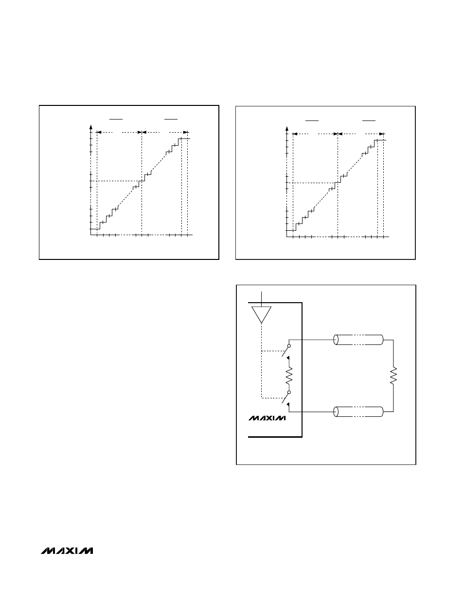
Double Termination (DT)
As shown in Figure 8, the MAX1127 offers an optional,
internal 100Ω termination between the differential output
pairs (OUT_P and OUT_N, CLKOUTP and CLKOUTN,
FRAMEP and FRAMEN). In addition to the termination
at the end of the line, a second termination directly at
the outputs helps eliminate unwanted reflections down
the line. This feature is useful in applications where
trace lengths are long (>5in) or with mismatched
impedance. Drive DT high to select double termination,
or drive DT low to disconnect the internal termination
resistor (single termination). Selecting double termina-
tion increases the OV
DD
supply current (see the
Electrical Characteristics table).
Power-Down Modes
The MAX1127 offers two types of power-down inputs,
PD0–PD3 and PDALL. The power-down modes allow
the MAX1127 to use power efficiently by transitioning to
a low-power state when conversions are not required.
Independent Channel Power-Down (PD0–PD3)
PD0–PD3 control the power-down mode of each chan-
nel independently. Drive a power-down input high to
power down its corresponding input channel. For exam-
ple, to power down channel 1, drive PD1 high. Drive a
power-down input low to place the corresponding input
channel in normal operation. The differential output
impedance of a powered-down output channel is
approximately 378Ω, when DT is low. The output imped-
ance of OUT_P, with respect to OUT_N, is 100Ω when
DT is high. See the Electrical Characteristics table for
typical supply currents with powered-down channels.
The state of the internal reference is independent of the
PD0–PD3 inputs. To power down the internal reference
circuitry, drive PDALL high (see the Global Power-
Down (PDALL) section).
DIFFERENTIAL INPUT VOLTAGE (LSB)
-2045
+2047
+2045
-1 0 +1
-2047
0x800
0x801
0x802
0x803
0x7FF
0x7FE
0x7FD
0xFFF
0x000
0x001
FSR
FSR
1 LSB =2 x FSR
4096
FSR = 700mV x VREFIO
1.24V
TWO'S COMPLEMENT OUTPUT CODE (LSB)
Figure 6. Bipolar Transfer Function with Two’s Complement
Output Code (
T
/B = 0)
DIFFERENTIAL INPUT VOLTAGE (LSB)
-2045
+2047
+2045
-1 0 +1
-2047
0x000
0x800
0x002
0x003
0xFFF
0xFFE
0xFFD
0x7FF
0x800
0x801
FSR
FSR
1 LSB =2 x FSR
4096
FSR = 700mV x VREFIO
1.24V
OFFSET BINAR
Y OUTPUT CODE (LSB)
Figure 7. Bipolar Transfer Function with Offset Binary Output
Code (
T
/B = 1)
MAX1127
100Ω
100Ω
OUT_P/
CLKOUTP/
FRAMEP
OUT_N/
CLKOUTN/
FRAMEN
DT
SWITCHES ARE CLOSED WHEN DT IS HIGH.
SWITCHES ARE OPEN WHEN DT IS LOW.
Z
0
= 50Ω
Z
0
= 50Ω
Figure 8. Double Termination