Table 2. output code table (v, 24v), Lvds – Rainbow Electronics MAX1127 User Manual
Page 20: Refio
MAX1127
Quad, 12-Bit, 65Msps, 1.8V ADC with
Serial LVDS Outputs
20
______________________________________________________________________________________
Frame Alignment Output (FRAMEP, FRAMEN)
The MAX1127 provides a differential frame alignment
signal that consists of FRAMEP and FRAMEN. As shown
in Figure 4, the rising edge of the frame alignment sig-
nal corresponds to the first bit (D0) of the 12-bit serial
data stream. The frequency of the frame alignment sig-
nal is identical to the frequency of the sample clock.
Serial Output Data (OUT_P, OUT_N)
The MAX1127 provides its conversion results through
individual differential outputs consisting of OUT_P and
OUT_N. The results are valid 6.5 input clock cycles
after the sample is taken. As shown in Figure 3, the out-
put data is clocked out on both edges of the output
clock, LSB (D0) first. Figure 5 provides the detailed ser-
ial output timing diagram.
Output Data Format (
T
/B), Transfer Functions
The MAX1127 output data format is either offset binary or
two’s complement, depending on the logic input T/B.
With T/B low, the output data format is two’s comple-
ment. With T/B high, the output data format is offset bina-
ry. The following equations, Table 2, Figure 6, and Figure
7 define the relationship between the digital output and
the analog input. For two’s complement (T/B = 0):
and for offset binary (T/B = 1):
where CODE
10
is the decimal equivalent of the digital
output code as shown in Table 2. FSR is the full-scale
range as shown in Figures 6 and 7.
Keep the capacitive load on the MAX1127 digital out-
puts as low as possible.
LVDS and SLVS Signals (SLVS/
LVDS
)
Drive SLVS/LVDS low for LVDS or drive SLVS/LVDS
high for scalable low-voltage signaling (SLVS) levels at
the MAX1127 outputs (OUT_P, OUT_N, CLKOUT_P,
CLKOUT_N, FRAMEP_, and FRAMEN_). See the
Electrical Characteristics table for LVDS and SLVS out-
put voltage levels.
LVDS Test Pattern (LVDSTEST)
Drive LVDSTEST high to enable the output test pattern
on all LVDS or SLVS output channels. The output test
pattern is 0000 1011 1101 MSB→LSB. As with the ana-
log conversion results, the test pattern data is output
LSB first. Drive LVDSTEST low for normal operation
(test pattern disabled).
V
V
FSR
CODE
IN P
IN N
_
_
−
=
Ч Ч
−
2
2048
4096
10
V
V
FSR
CODE
IN P
IN N
_
_
−
=
Ч Ч
2
4096
10
(V
CLKOUTP
-
V
CLKOUTN
)
(V
OUT_P
-
V
OUT_N
)
t
CH
t
CL
t
OD
t
OD
D0
D1
D2
D3
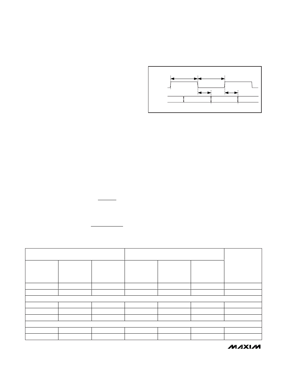
Figure 5. Serialized Output Detailed Timing Diagram
TWO’S COMPLEMENT DIGITAL OUTPUT CODE
(
T
/B = 0)
OFFSET BINARY DIGITAL OUTPUT CODE
(
T
/B = 1)
BINARY
D11
D0
HEXADECIMAL
EQUIVALENT
OF
D11
D0
DECIMAL
EQUIVALENT
OF
D11
D0
BINARY
D11
D0
HEXADECIMAL
EQUIVALENT
OF
D11
D0
DECIMAL
EQUIVALENT
OF
D11
D0
V
IN_P
- V
IN_P
(mV)
(V
REFIO
= 1.24V)
0111 1111 1111
0x7FF
+2047
1111 1111 1111
0xFFF
+4095
+699.66
0111 1111 1110
0x7FE
+2046
1111 1111 1110
0xFFE
+4094
+699.32
0000 0000 0001
0x001
+1
1000 0000 0001
0x801
+2049
+0.34
0000 0000 0000
0x000
0
1000 0000 0000
0x800
+2048
0
1111 1111 1111
0xFFF
-1
0111 1111 1111
0x7FF
+2047
-0.34
1000 0000 0001
0X801
-2047
0000 0000 0001
0x001
+1
-699.66
1000 0000 0000
0x800
-2048
0000 0000 0000
0x000
0
-700.00
Table 2. Output Code Table (V
REFIO
= 1.24V)