Table 1. pll2 and pll3 configuration – Rainbow Electronics MAX1127 User Manual
Page 18
MAX1127
Quad, 12-Bit, 65Msps, 1.8V ADC with
Serial LVDS Outputs
18
______________________________________________________________________________________
Reference Configurations
(REFIO and
INTREF
)
The MAX1127 provides an internal 1.24V bandgap ref-
erence or can be driven with an external reference volt-
age. The MAX1127 full-scale analog differential input
range is ±FSR. Full-scale range (FSR) is given by the
following equation:
where V
REFIO
is the voltage at REFIO, generated inter-
nally or externally. For a V
REFIO
= 1.24V, the full-scale
input range is ±700mV (1.4V
P-P
).
Internal Reference Mode
Connect INTREF to GND to use the internal bandgap
reference directly. The internal bandgap reference gen-
erates REFIO to be 1.24V with a 100ppm/°C tempera-
ture coefficient in internal reference mode. Connect an
external ≥0.1µF bypass capacitor from REFIO to GND
for stability. REFIO sources up to 200µA and sinks up
to 200µA for external circuits, and REFIO has a load
regulation of 83mV/mA. The global power-down input
(PDALL) enables and disables the reference circuit.
REFIO has >1MΩ resistance to GND when the
MAX1127 is in power-down mode. The internal refer-
ence circuit requires 132µs to power-up and settle
when power is applied to the MAX1127 or when PDALL
transitions from high to low.
External Reference Mode
The external reference mode allows for more control
over the MAX1127 reference voltage and allows multi-
ple converters to use a common reference. Connect
INTREF to AV
DD
to disable the internal reference and
enter external reference mode. Apply a stable 1.24V
source at REFIO. Bypass REFIO to GND with a 0.1µF
capacitor. The REFIO input impedance is >1MΩ.
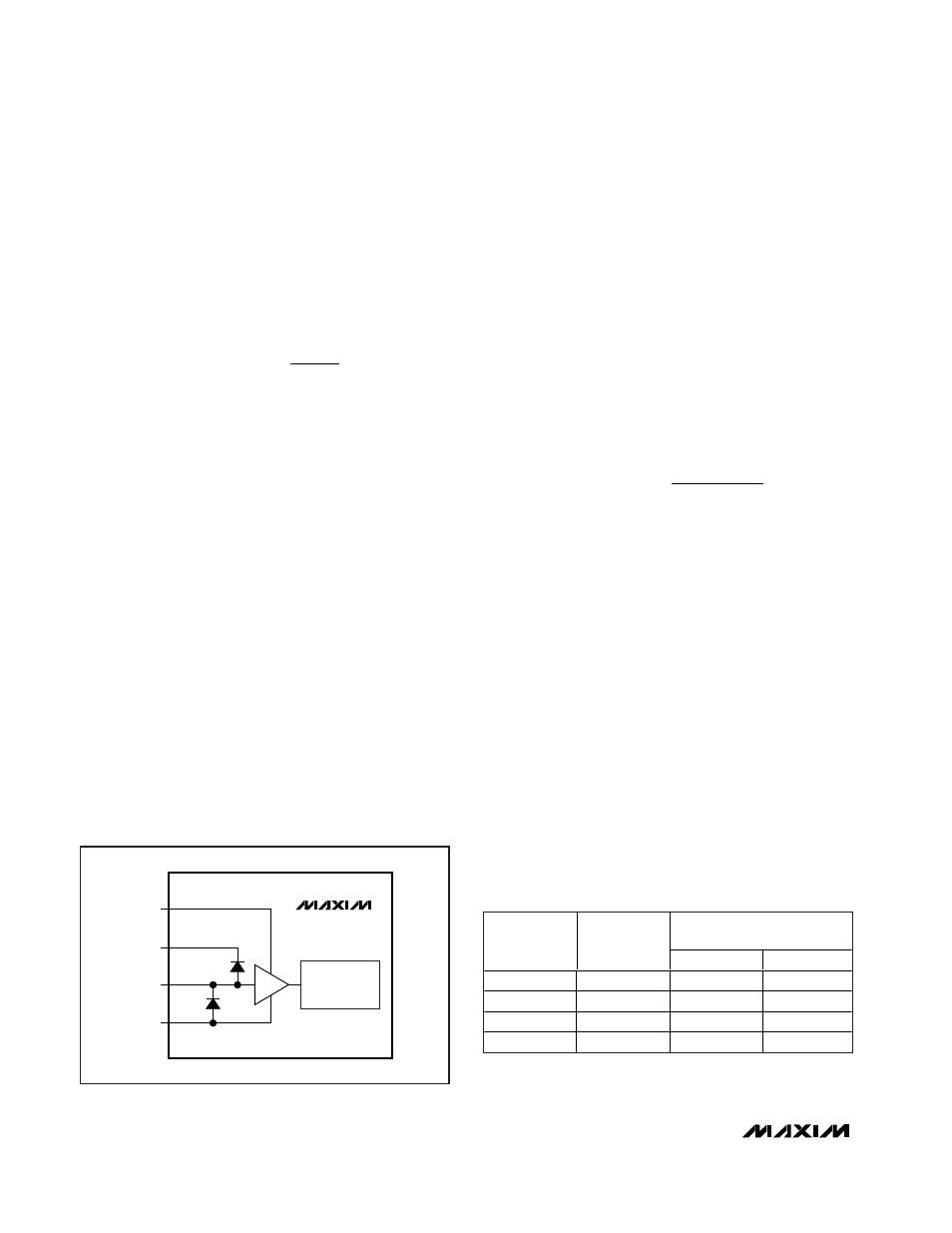
Clock Input (CLK)
The MAX1127 accepts a CMOS-compatible clock sig-
nal with a wide 20% to 80% input-clock duty cycle.
Drive CLK with an external single-ended clock signal.
Figure 2 shows the simplified clock input diagram.
Low clock jitter is required for the specified SNR perfor-
mance of the MAX1127. Analog input sampling occurs
on the rising edge of CLK, requiring this edge to pro-
vide the lowest possible jitter. Jitter limits the maximum
SNR performance of any ADC according to the follow-
ing relationship:
where f
IN
represents the analog input frequency and t
J
is the total system clock jitter. Clock jitter is especially
critical for undersampling applications. For example,
assuming that clock jitter is the only noise source, to
obtain the specified 69.4dB of SNR with an input fre-
quency of 30.3MHz, the system must have less than
1.8ps of clock jitter. In actuality, there are other noise
sources, such as thermal noise and quantization noise,
that contribute to the system noise requiring the clock
jitter to be less than 0.5ps to obtain the specified
69.4dB of SNR at 30.3MHz.
The MAX1127 features a PLL that generates an output
clock signal with six times the frequency of the input
clock. The output clock signal is used to clock data out
of the MAX1127 (see the System Timing Requirements
section). Set the PLL2 and PLL3 bits according to the
input clock range provided in Table 1. PLL0 and PLL1
are reserved for factory testing and must always be
connected to GND.
SNR
f
t
IN
J
=
Ч
Ч Ч
Ч
20
1
2
log
π
FSR
mV
V
V
REFIO
=
×
700
1 24
.
MAX1127
DUTY-CYCLE
EQUALIZER
AV
DD
CV
DD
CLK
GND
Figure 2. Clock Input Circuitry
CLOCK INPUT RANGE
(MHz)
PLL2
PLL3
MIN
MAX
0
0
48.750
65.000
0
1
32.500
48.750
1
0
24.375
32.500
1
1
16.000
24.375
Table 1. PLL2 and PLL3 Configuration
*PLL0 and PLL11 are reserved for factory testing and must
always be connected to GND.