Functional diagram, Pin description (continued) – Rainbow Electronics MAX1127 User Manual
Page 16
MAX1127
Quad, 12-Bit, 65Msps, 1.8V ADC with
Serial LVDS Outputs
16
______________________________________________________________________________________
LVDS/SLVS
OUTPUT
DRIVERS
REFERENCE
SYSTEM
PLL
6x
CLOCK
CIRCUITRY
POWER CONTROL
REFIO
INTREF
IN0P
IN0N
IN1P
IN1N
IN2P
IN2N
IN3P
IN3N
CLK
PDALL PD0
PD1
PD2
PD3
OUT0P
OUT0N
OUT1P
OUT1N
OUT2P
OUT2N
OUT3P
OUT3N
CLKOUTP
CLKOUTN
OV
DD
AV
DD
GND
CV
DD
PLL3
PLL0 PLL1 PLL2
T/B
LVDSTEST
FRAMEP
FRAMEN
DT
OUTPUT
CONTROL
MAX1127
T/H
12-BIT
PIPELINE
ADC
12:1
SERIALIZER
T/H
12-BIT
PIPELINE
ADC
12:1
SERIALIZER
T/H
12-BIT
PIPELINE
ADC
12:1
SERIALIZER
T/H
12-BIT
PIPELINE
ADC
12:1
SERIALIZER
SLVS/LVDS
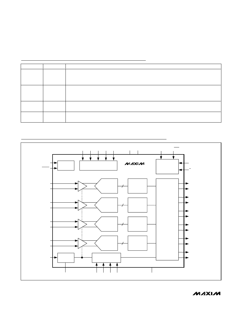
Functional Diagram
PIN
NAME
FUNCTION
64
LVDSTEST
LVDS Test Pattern Enable Input. Drive LVDSTEST high to enable the output test pattern
(000010111101 MSB
→
LSB). As with the analog conversion results, the test pattern data is output
LSB first. Drive LVDSTEST low for normal operation.
66
REFIO
Reference Input/Output. For internal reference operation (INTREF = GND), the reference output
voltage is 1.24V. For external reference operation (INTREF = AV
DD
), apply a stable reference voltage
at REFIO. Bypass to GND with a 0.1µF capacitor.
67
INTREF
Internal/External Reference Mode Select Input. For internal reference mode, connect INTREF directly
to GND. For external reference mode, connect INTREF directly to AV
DD
.
—
EP
Exposed Paddle. EP is internally connected to GND. Externally connect EP to GND to achieve
specified performance.
Pin Description (continued)