Max1338, Gain error, Signal-to-noise ratio (snr) – Rainbow Electronics MAX1338 User Manual
Page 20
MAX1338
Gain Error
Gain error indicates how well the slope of the actual
transfer function matches the slope of the ideal transfer
function. For the MAX1338, the gain error is the differ-
ence between the measured positive full-scale and
negative full-scale transition points minus the difference
between the ideal positive full-scale and negative full-
scale bipolar transition points.
Signal-to-Noise Ratio (SNR)
SNR is a measure of the converter’s noise characteris-
tics. For a waveform perfectly reconstructed from digi-
tal samples, SNR is the ratio of the full-scale analog
input (RMS value) to the RMS quantization error (resid-
ual error). The ideal, theoretical minimum analog-to-dig-
ital noise is caused by quantization noise error only and
results directly from the ADC’s resolution (N bits):
14-Bit, 4-Channel, Software-Programmable,
Multiranging, Simultaneous-Sampling ADC
20
______________________________________________________________________________________
4 x V
REFADC
4 x V
REF
2
14
1 LSB =
TWO'S COMPLEMENT BINAR
Y OUTPUT CODE
-8192 -8190
+8191
+8189
0x2000
0x2001
0x2002
0x2003
0x1FFF
0x1FFE
0x1FFD
0x1FFC
0x3FFF
0x0000
0x0001
0
INPUT VOLTAGE (V
AIN_+
- V
AIN_-
IN LSBs)
-1
+1
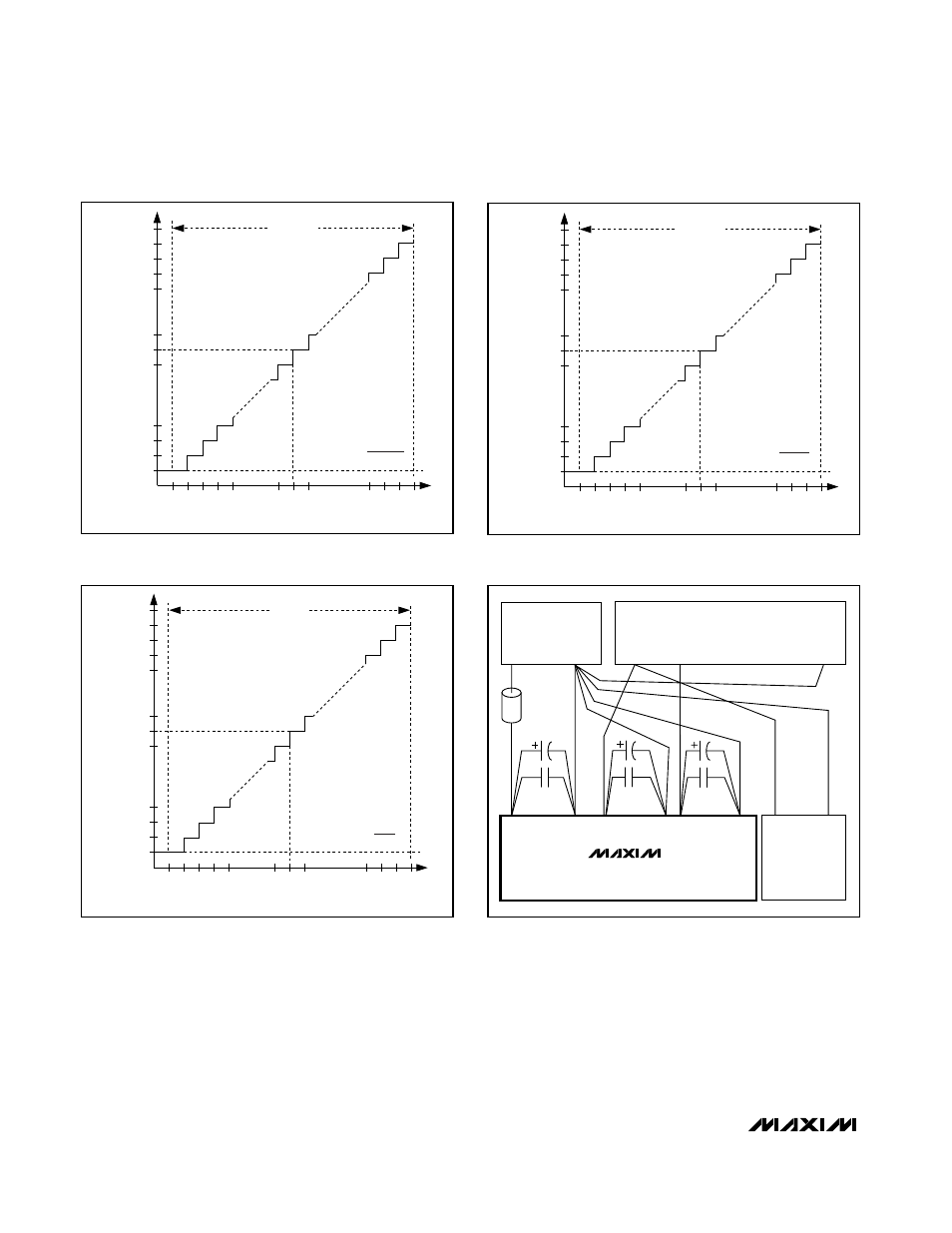
Figure 9. ±5V Transfer Function
2 x V
REFADC
2 x V
REF
2
14
1 LSB =
TWO'S COMPLEMENT BINAR
Y OUTPUT CODE
-8192 -8190
+8191
+8189
0x2000
0x2001
0x2002
0x2003
0x1FFF
0x1FFE
0x1FFD
0x1FFC
0x3FFF
0x0000
0x0001
0
INPUT VOLTAGE (V
AIN_+
- V
AIN_-
IN LSBs)
-1
+1
Figure 10. ±2.5V Transfer Function
V
REFADC
V
REF
2
14
1 LSB =
TWO'S COMPLEMENT BINAR
Y OUTPUT CODE
-8192 -8190
+8191
+8189
0x2000
0x2001
0x2002
0x2003
0x1FFF
0x1FFE
0x1FFD
0x1FFC
0x3FFF
0x0000
0x0001
0
INPUT VOLTAGE (V
AIN_+
- V
AIN_-
IN LSBs)
-1
+1
Figure 11. ±1.25V Transfer Function
DIGITAL POWER SUPPLIES
AV
DD
AGND
DGND
+5V
DIGITAL
CIRCUITS
FERRITE
BEAD
+5V
DV
DD
GND
MAX1338
+5V
+3V
GND
AGND
ANALOG
POWER SUPPLY
DRV
DD
DRGND
Figure 12. Power-Supply Grounding and Bypassing