Max1338, Applications information – Rainbow Electronics MAX1338 User Manual
Page 18
MAX1338
Input Range Settings
Table 4 shows the two’s complement output for a selec-
tion of inputs.
The full-scale input range (FSR) depends on the select-
ed range, and the voltage at REF, as shown in Table 5.
Also shown in Table 5 are the allowable common-mode
ranges for the differential inputs.
Calculate the LSB size using:
where A = gain multiplier for the selected input range,
from Table 6.
Determine the input voltage as a function of V
REF
, and
the output code using:
where A = gain multiplier for the selected input range,
from Table 6.
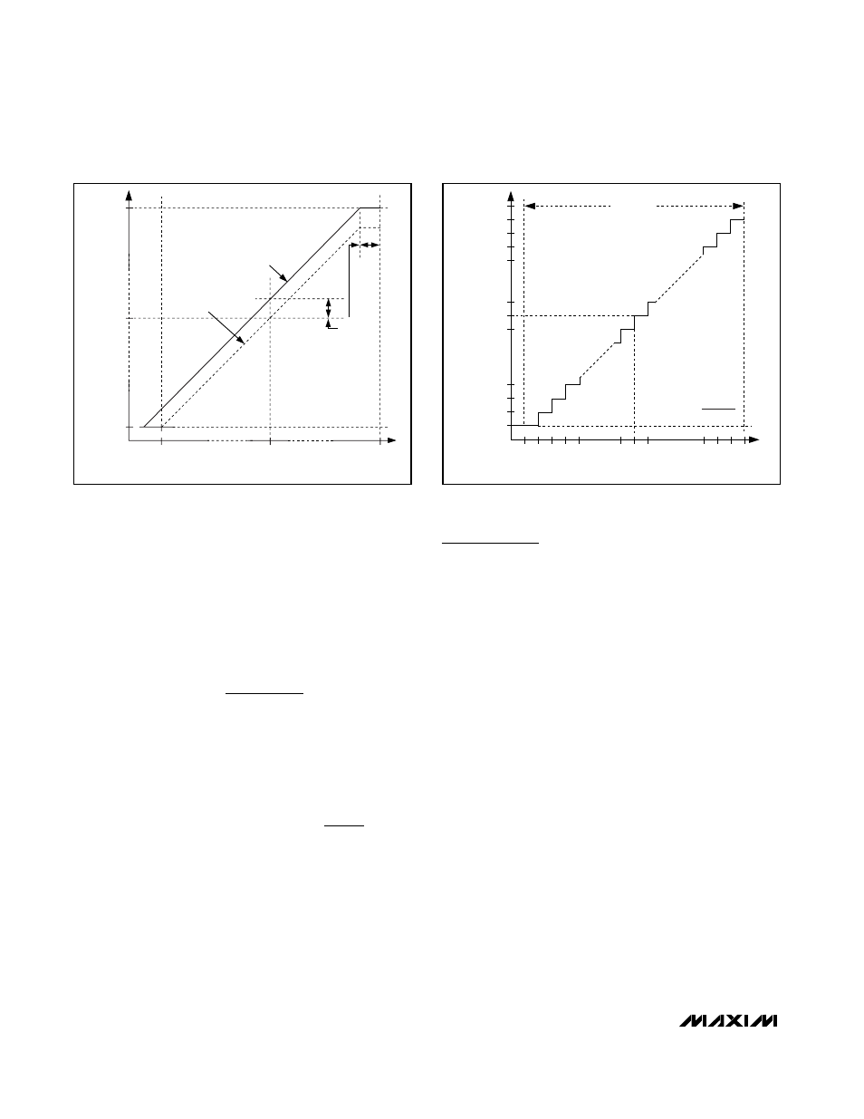
Figures 8, 9, 10, and 11 show the transfer functions for
the four selectable input ranges.
Applications Information
Layout, Grounding, and Bypassing
For best performance, the board layout must follow
some simple guidelines. Separate the control I/O and
parallel I/O signals from the analog signals, and run the
clock signals separate from everything. Do not run ana-
log and digital (especially clock) lines parallel to one
another, or digital lines underneath the ADC package.
Run the parallel I/O signals together as a bundle.
The MAX1338 has an exposed underside pad for a
low-inductance ground connection and low thermal
resistance. Connect the exposed pad to the circuit
board ground plane. Figure 12 shows the recommend-
ed system ground connections. Establish an analog
ground point at AGND and a digital ground point at
DGND. Connect all analog grounds to the analog
ground point. Connect all digital grounds to the digital
ground point. For lowest noise operation, make the
power-supply ground returns as low impedance and as
short as possible. Connect the analog ground point to
the digital ground point at one location.
High-frequency noise in the power supplies degrades
the ADC’s performance. Bypass AV
DD
to AGND with a
parallel combination of 0.1µF and 2.2µF capacitors,
bypass DV
DD
to DGND with a parallel combination of
0.1µF and 2.2µF capacitors, and bypass DRV
DD
to
DRGND with a parallel combination of 0.1µF and 2.2µF
capacitors. If the supply is very noisy use a ferrite bead
as a lowpass filter, as shown in Figure 12.
V
V
V
A
CODE
AIN
AIN
REFADC
_
_
+
−
−
=
Ч
Ч
2
14
1
2
14
LSB
A V
REFADC
=
×
14-Bit, 4-Channel, Software-Programmable,
Multiranging, Simultaneous-Sampling ADC
18
______________________________________________________________________________________
MAXIMUM
64 CODES
+8191
0
-8192
0x2000
0x0000
0x1FFF
OUTPUT CODE
ADJUSTED
TRANSFER
FUNCTION
INITIAL
TRANSFER
FUNCTION
INPUT VOLTAGE (LSBs)
Figure 7. Example of Digitally Adjusted Transfer Function—
Shifted Down to Minimize Zero-Code Offset
8 x V
REFADC
8 x V
REF
2
14
1 LSB =
TWO'S COMPLEMENT BINAR
Y OUTPUT CODE
-8192 -8190
+8191
+8189
0x2000
0x2001
0x2002
0x2003
0x1FFF
0x1FFE
0x1FFD
0x1FFC
0x3FFF
0x0000
0x0001
0
INPUT VOLTAGE (V
AIN_+
- V
AIN_-
IN LSBs)
-1
+1
Figure 8. ±10V Transfer Function