Rainbow Electronics MAX1338 User Manual
Page 13
Power-Supply Inputs
Three separate power supplies power the MAX1338. A
+5V analog supply, AV
DD
, powers the analog input and
converter sections. A +5V digital supply, DV
DD
, powers
the internal logic circuitry, and a +2.7V to +5V digital
supply (DRV
DD
), powers the parallel I/O and the control
I/O (see the Typical Operating Circuit). Bypass the
power supplies as indicated in the Layout, Grounding,
and Bypassing section. Power-supply sequencing is
not required for the MAX1338.
Analog Inputs
Software-Selectable Input Range
The MAX1338 provides four independent, software-
selectable, analog input voltage ranges for each chan-
nel. The selectable input ranges are ±V
REF
x 4 (the
power-up default condition), ±V
REF
x 2, ±V
REF
, and
±V
REF
x 0.5. Using the 2.5V internal reference, the
selectable input ranges are ±10V (power-up default),
±5V, ±2.5V, and ±1.25V. Program the analog input
ranges with the configuration register through the
parallel I/O. See the Configuration Register section for
programming details.
Input Protection
Protection at the analog inputs provides ±17V fault
immunity for the MAX1338. This protection circuit limits
the current at the analog inputs to less than ±2mA.
Input fault protection is active in standby, in shutdown,
during normal operation, and over all input ranges.
Track and Hold (T/H)
To preserve relative phase information between input
channels, each input channel has a dedicated T/H
amplifier. The rising edge of CONVST represents the
sampling instant for all channels. All samples are taken
within an aperture delay (t
AD
) of 16ns. The aperture
delay of all channels is matched to within 100ps.
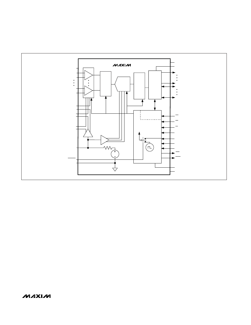
MAX1338
14-Bit, 4-Channel, Software-Programmable,
Multiranging, Simultaneous-Sampling ADC
______________________________________________________________________________________
13
MAX1338
CONVST
D13
DGND
AV
DD
SHDN
CLK
INTERFACE
AND
CONTROL
14-BIT
ADC
D0
DV
DD
AGND
STANDBY
REFADC
S/H
4 x 14
SRAM
OUTPUT
DRIVERS
5kΩ
2.500V
INTCLK/EXTCLK
CS
RD
EOC
EOLC
REFN1
DRGND
WR
DRV
DD
D8
D7
CONFIGURATION
REGISTER
REFN2
COM1
COM2
REFP2
REFP1
AIN3+
AIN3-
S/H
AIN0-
AIN0+
4 x 1
MUX
Figure 2. Functional Diagram