Table 1. configuration register, Table 2. input-range register settings – Rainbow Electronics MAX1338 User Manual
Page 15
External Clock
For external clock operation, force INTCLK/EXTCLK low
and connect an external clock source to CLK. Use an
external clock frequency from 1MHz to 6MHz with a
duty cycle between 40% and 60%. Choose a minimum
clock frequency of 1MHz to prevent linearity errors
caused by excessive droop in the T/H circuits.
Applications Sections
Power-On Reset
At power-up, all channels default to a ±10V input range.
After applying power, allow a 1ms wake-up time to
elapse and perform one dummy conversion before
initiating first conversion.
Power Saving
Full Shutdown
During shutdown, the analog and digital circuits in the
MAX1338 power down and the device draws less than
0.06mA from AV
DD
, and less than 10µA from DV
DD
.
Select shutdown mode using the SHDN input. Force
SHDN high to enter shutdown mode. When coming out of
shutdown, allow the 1ms wake-up and then perform one
dummy conversion before making the first conversion.
Standby
Standby is similar to shutdown but the reference cir-
cuits remain powered up, allowing faster wake-up.
Enter standby by forcing STANDBY high. After coming
out of standby, perform a dummy conversion before
making the first conversion.
Digital Interface
The digital interface consists of two sections: a control
I/O section and a parallel I/O section. The control I/O
section includes the following control signals: chip
select (CS), read (RD), write (WR), end of conversion
(EOC), end of last conversion (EOLC), convert start
(CONVST), power-down (SHDN), standby (STANDBY),
and external-clock input (CLK).
The bidirectional parallel I/O section sets the 8-bit input
range configuration register using D0–D7 (see the
Configuration Register section) and outputs the 14-bit
conversion result using D0–D13. The I/O operations are
controlled by the control I/O signals RD, WR, and CS. All
parallel I/O bits are high impedance when either RD = 1
or CS = 1. Figures 4, 5, and 6 and the Timing Character-
istics section detail the operation of the digital interface.
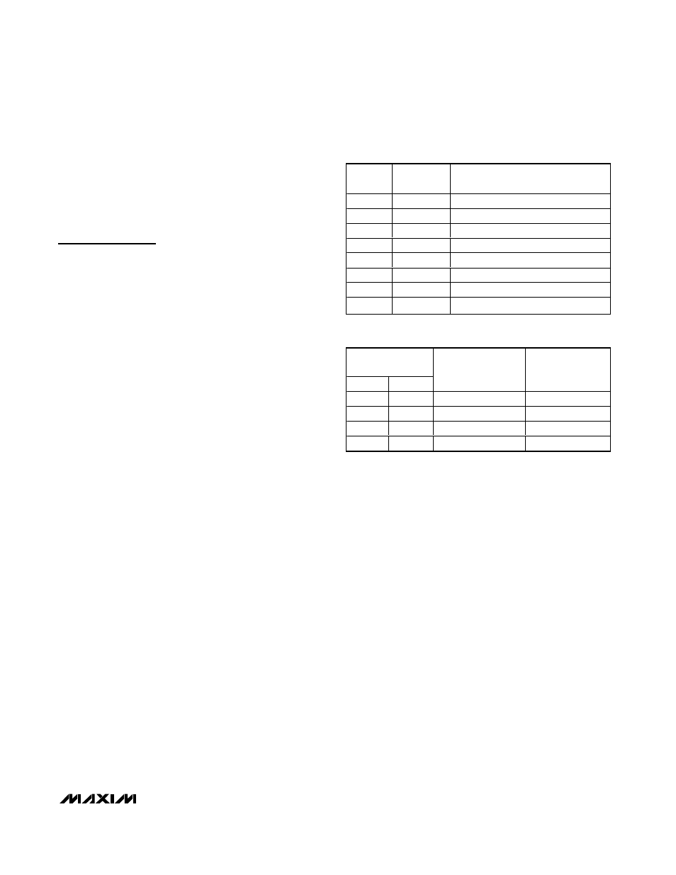
Configuration Register
The MAX1338 uses an 8-bit configuration word to set the
input range for each channel. Table 1 and Table 2 describe
the configuration word and the input-range settings.
Write to the configuration register by forcing CS and WR
low, loading bits D0–D7 onto the parallel bus, and then
forcing WR high. The configuration bits are latched on
the rising edge of WR (Figure 4). It is possible to write to
the configuration register at any point during the conver-
sion sequence. However, it will not be active until the
next convert-start signal. At power-up, the configuration
register contains all zeros, making all channels default to
the maximum input range, -10V to +10V. Shutdown and
standby do not change the configuration register, but
the configuration register can be programmed while the
MAX1338 is in shutdown or standby modes.
MAX1338
14-Bit, 4-Channel, Software-Programmable,
Multiranging, Simultaneous-Sampling ADC
______________________________________________________________________________________
15
I/O LINE
REGISTER
NAME
FUNCTION
D0
CH0R0
Channel 0 input range setting bit 0
D1
CH0R1
Channel 0 input range setting bit 1
D2
CH1R0
Channel 1 input range setting bit 0
D3
CH1R1
Channel 1 input range setting bit 1
D4
CH2R0
Channel 2 input range setting bit 0
D5
CH2R1
Channel 2 input range setting bit 1
D6
CH3R0
Channel 3 input range setting bit 0
D7
CH3R1
Channel 3 input range setting bit 1
Table 1. Configuration Register
REGISTER
SETTING
CH_R0
CH_R1
SELECTED INPUT
RANGE
ALLOWABLE
COMMON-MODE
RANGE
0
0
-10V to +10V
±5V
0
1
-5V to +5V
±2.5V
1
0
-2.5V to +2.5V
±1.25V
1
1
-1.25V to +1.25V
±0.625V
Table 2. Input-Range Register Settings