Max1338 – Rainbow Electronics MAX1338 User Manual
Page 14
MAX1338
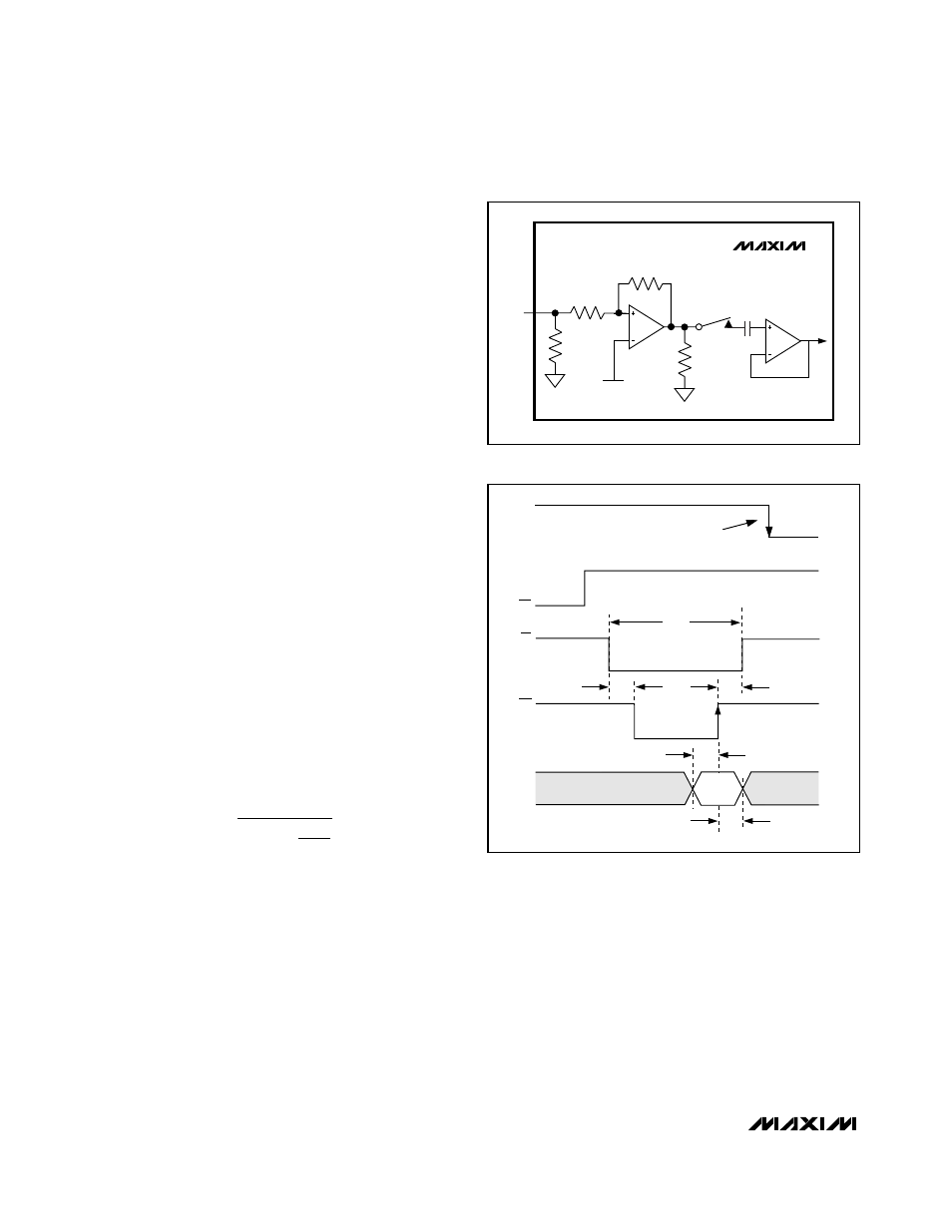
Figure 3 shows the equivalent analog input T/H circuit
for one analog input.
As conversion begins, the T/H circuits hold the analog
signals. After the 12th clock cycle (or 2.4µs in internal
clock mode) into the conversion process, the last ana-
log input sample begins shifting through the converter,
and the T/H circuits begin to track the analog inputs
again in preparation for the next CONVST rising edge.
Due to the resistive load presented by the analog
inputs, any significant analog input source resistance,
R
SOURCE
, increases gain error. Limit R
SOURCE
to a
maximum of 20Ω to limit the effect to less than 0.1%.
Drive the input with a wideband buffer (>1MHz) that
can drive the ADC’s input impedance.
Selecting an Input Buffer
Most applications require an input buffer to achieve 14-
bit accuracy. Although slew rate and bandwidth are
important, the most critical specification is output imped-
ance. Use a low-noise, low-distortion amplifier with low
output impedance, for best gain-accuracy performance.
Input Bandwidth
The input-tracking circuitry has a 1MHz small-signal
bandwidth. To avoid high-frequency signals being
aliased into the frequency band of interest, anti-alias fil-
tering is recommended.
Data Throughput
The data throughput (f
TH
) of the MAX1338 is a function
of the clock speed (f
CLK
). The MAX1338 operates from
a 5MHz internal clock or an external clock between
1MHz and 6MHz. For fastest throughput, read the con-
version result during conversion (Figure 5), and calcu-
late data throughput using:
where t
QUIET
is the period of bus inactivity before the
rising edge of CONVST.
Clock Modes
The MAX1338 provides an internal clock of 5MHz.
Alternatively, use an external clock of 1MHz to 6MHz.
Internal Clock
Internal clock mode frees the microprocessor from the
burden of running the ADC conversion clock. For inter-
nal-clock operation, connect INTCLK/EXTCLK to AV
DD
and CLK to DRGND. Note that INTCLK/EXTCLK is ref-
erenced to the analog power supply, AV
DD
. Total con-
version time for all four channels using the internal
clock is 6µs (typ).
f
t
f
TH
QUIET
CLK
=
+
1
26
14-Bit, 4-Channel, Software-Programmable,
Multiranging, Simultaneous-Sampling ADC
14
______________________________________________________________________________________
AIN_
R1
MAX1338
R2
1.9V
R1 || R2 = 6.25kΩ
C
HOLD
Figure 3. Simplified Typical Input Circuit
t
CS
t
CTW
t
WRL
t
WTC
t
DTW
DATA
IN
t
WTD
CONVST
CONFIGURATION
REGISTER ACTIVATES
RD
CS
WR
D0–D7
Figure 4. Write Timing