Grounding, bypassing, and board layout – Rainbow Electronics MAX1183 User Manual
Page 15
quadrature (Q) carrier component, where the Q compo-
nent is 90-degree phase-shifted with respect to the in-
phase component. At the receiver, the QAM signal is
divided down into its I and Q components, essentially
representing the modulation process reversed. Figure 8
displays the demodulation process performed in the
analog domain, using the dual matched +3V, 10-bit
ADC MAX1183 and the MAX2451 quadrature demodu-
lator to recover and digitize the I and Q baseband sig-
nals. Before being digitized by the MAX1183, the
mixed-down signal components may be filtered by
matched analog filters, such as Nyquist or pulse-shap-
ing filters, which remove any unwanted images from the
mixing process, thereby enhancing the overall SNR
performance and minimizing intersymbol interference.
Grounding, Bypassing, and
Board Layout
The MAX1183 requires high-speed board layout design
techniques. Locate all bypass capacitors as close to
the device as possible, preferably on the same side as
the ADC, using surface-mount devices for minimum
inductance. Bypass V
DD
, REFP, REFN, and COM with
two parallel 0.1µF ceramic capacitors and a 2.2µF
bipolar capacitor to GND. Follow the same rules to
bypass the digital supply (OV
DD
) to OGND. Multilayer
boards with separated ground and power planes pro-
duce the highest level of signal integrity. Consider the
use of a split ground plane arranged to match the
physical location of the analog ground (GND) and the
digital output driver ground (OGND) on the ADC’s
package. The two ground planes should be joined at a
single point such that the noisy digital ground currents
do not interfere with the analog ground plane. The ideal
location of this connection can be determined experi-
mentally at a point along the gap between the two
ground planes, which produces optimum results. Make
this connection with a low-value, surface-mount resistor
MAX1183
Dual 10-Bit, 40Msps, +3V, Low-Power ADC with
Internal Reference and Parallel Outputs
______________________________________________________________________________________
15
MAX1183
T1
N.C.
V
IN
6
1
5
2
4
3
22pF
22pF
0.1
µF
0.1
µF
2.2
µF
25
Ω
25
Ω
MINICIRCUITS
TT1–6
T1
N.C.
V
IN
6
1
5
2
4
3
22pF
22pF
0.1
µF
0.1
µF
2.2
µF
25
Ω
25
Ω
MINICIRCUITS
TT1–6
INA-
INA+
INB-
INB+
COM
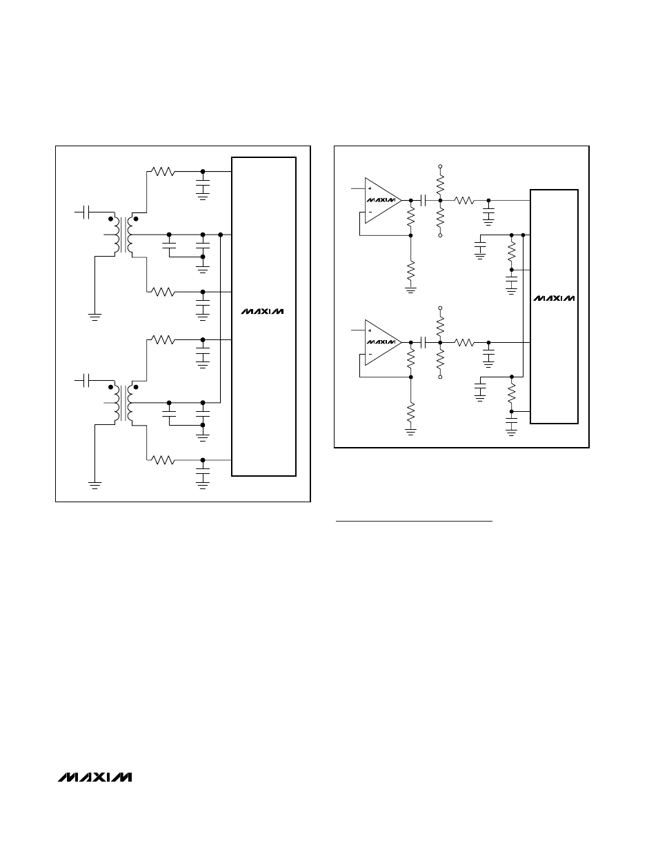
Figure 6. Transformer-Coupled Input Drive
MAX1183
0.1
µF
1k
Ω
1k
Ω
100
Ω
100
Ω
C
IN
22pF
C
IN
22pF
INB+
INB-
COM
INA+
INA-
0.1
µF
R
ISO
50
Ω
R
ISO
50
Ω
REFP
REFN
V
IN
MAX4108
0.1
µF
1k
Ω
1k
Ω
100
Ω
100
Ω
C
IN
22pF
C
IN
22pF
0.1
µF
R
ISO
50
Ω
R
ISO
50
Ω
REFP
REFN
V
IN
MAX4108
Figure 7. Using an Op Amp for Single-Ended, AC-Coupled
Input Drive