Max1183, Detailed description, Pin description (continued) – Rainbow Electronics MAX1183 User Manual
Page 10
MAX1183
Detailed Description
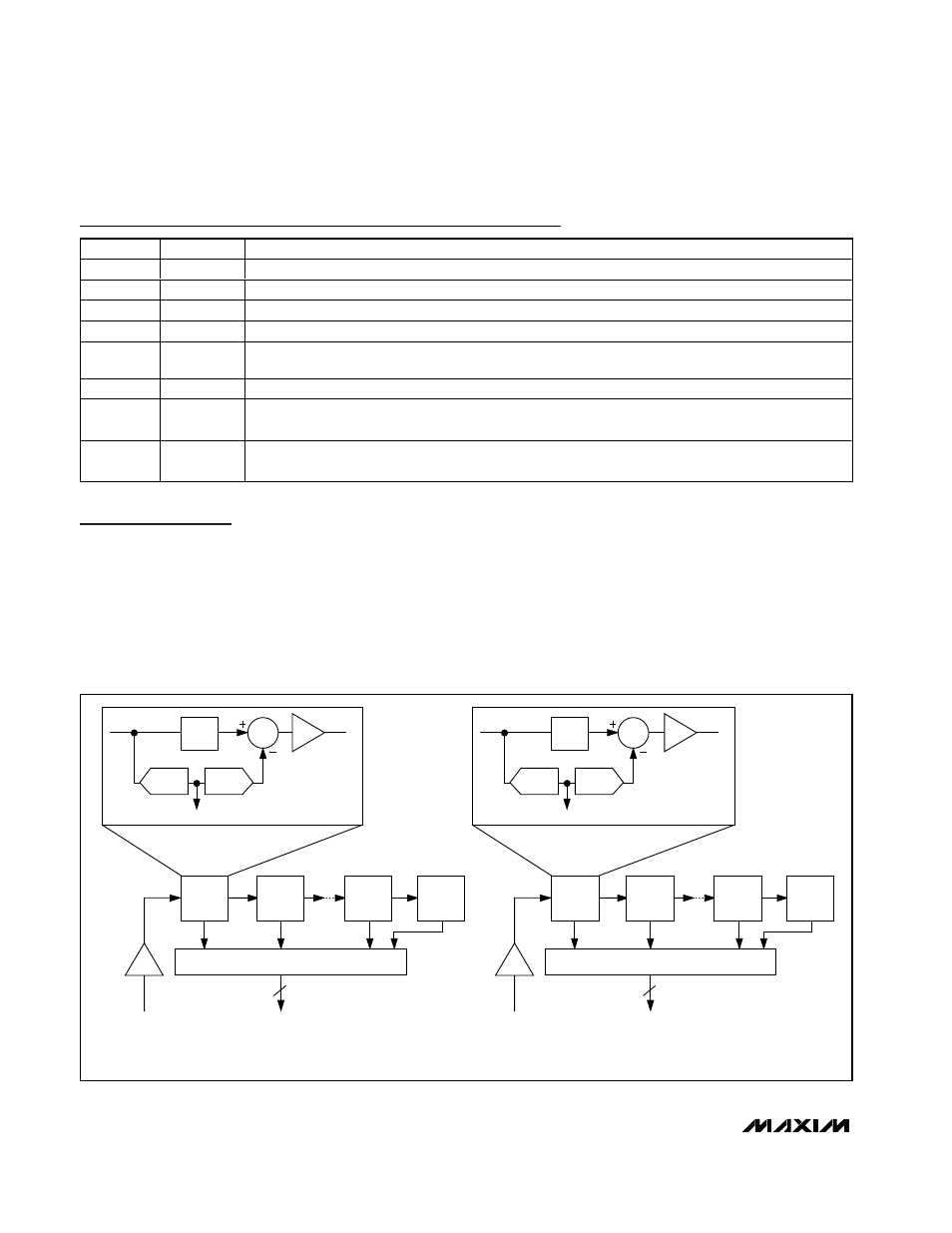
The MAX1183 uses a nine-stage, fully differential,
pipelined architecture (Figure 1) that allows for high-
speed conversion while minimizing power consump-
tion. Samples taken at the inputs move progressively
through the pipeline stages every half-clock cycle.
Including the delay through the output latch, the total
clock-cycle latency is five clock cycles.
One-and-a-half bit (2-comparator) flash ADCs convert
the held-input voltages into a digital code. The digital-
to-analog converters (DACs) convert the digitized
results back into analog voltages, which are then sub-
tracted from the original held-input signals. The result-
ing error signals are then multiplied by two, and the
residues are passed along to the next pipeline stages
where the process is repeated until the signals have
been processed by all nine stages. Digital error correc-
tion compensates for ADC comparator offsets in each
of these pipeline stages and ensures no missing
codes.
Dual 10-Bit, 40Msps, +3V, Low-Power ADC with
Internal Reference and Parallel Outputs
10
______________________________________________________________________________________
T/H
V
OUT
x2
Σ
FLASH
ADC
DAC
1.5 BITS
10
V
INA
V
IN
STAGE 1
STAGE 2
D9A–D0A
V
INA
= INPUT VOLTAGE BETWEEN INA+ AND INA- (DIFFERENTIAL OR SINGLE ENDED)
V
INB
= INPUT VOLTAGE BETWEEN INB+ AND INB- (DIFFERENTIAL OR SINGLE ENDED)
DIGITAL CORRECTION LOGIC
STAGE 8
STAGE 9
2-BIT FLASH
ADC
T/H
T/H
V
OUT
x2
Σ
FLASH
ADC
DAC
1.5 BITS
10
V
INB
V
IN
STAGE 1
STAGE 2
D9B–D0B
DIGITAL CORRECTION LOGIC
STAGE 8
STAGE 9
2-BIT FLASH
ADC
T/H
Figure 1. Pipelined Architecture—Stage Blocks
Pin Description (continued)
PIN
NAME
FUNCTION
41
D6A
Three-State Digital Output, Bit 6, Channel A
42
D7A
Three-State Digital Output, Bit 7, Channel A
43
D8A
Three-State Digital Output, Bit 8, Channel A
44
D9A
Three-State Digital Output, Bit 9 (MSB), Channel A
45
REFOUT
Internal Reference Voltage Output. May be connected to REFIN through a resistor or a resistor
divider.
46
REFIN
Reference Input. V
REFIN
= 2
✕
(V
REFP
- V
REFN
). Bypass to GND with a >1nF capacitor.
47
REFP
Positive Reference Input/Output. Conversion range is
±(V
REFP
- V
REFN
).
Bypass to GND with a > 0.1µF capacitor.
48
REFN
Negative Reference Input/Output. Conversion range is
±(V
REFP
- V
REFN
).
Bypass to GND with a > 0.1µF capacitor.