Applications information – Rainbow Electronics MAX1183 User Manual
Page 13

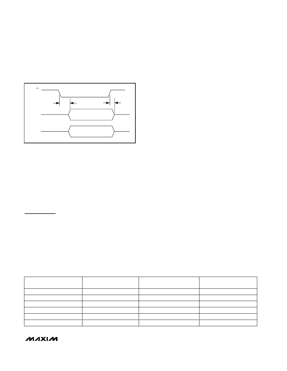
Figure 4 displays the timing relationship between out-
put enable and data output valid, as well as power-
down/wake-up and data output valid.
Power-Down (PD) and Sleep
(SLEEP) Modes
The MAX1183 offers two power-save modes—sleep
and full power-down modes. In sleep mode (SLEEP =
1), only the reference bias circuit is active (both ADCs
are disabled), and current consumption is reduced to
2.8mA. To enter full power-down mode, pull PD high.
With OE simultaneously low, all outputs are latched at
the last value prior to the power-down. Pulling OE high
forces the digital outputs into a high-impedance state.
Applications Information
Figure 5 depicts a typical application circuit containing
two single-ended to differential converters. The internal
reference provides a V
DD
/2 output voltage for level-
shifting purposes. The input is buffered and then split
to a voltage follower and inverter. One lowpass filter per
ADC suppresses some of the wideband noise associat-
ed with high-speed operational amplifiers, follows the
amplifiers. The user may select the R
ISO
and C
IN
val-
ues to optimize the filter performance to suit a particular
application. For the application in Figure 5, a R
ISO
of
50
Ω is placed before the capacitive load to prevent
ringing and oscillation. The 22pF C
IN
capacitor acts as
a small bypassing capacitor.
Using Transformer Coupling
An RF transformer (Figure 6) provides an excellent
solution to convert a single-ended source signal to a
fully differential signal, required by the MAX1183 for
optimum performance. Connecting the center tap of the
transformer to COM provides a V
DD
/2 DC level shift to
the input. Although a 1:1 transformer is shown, a step-
up transformer may be selected to reduce the drive
requirements. A reduced signal swing from the input
driver, such as an op amp, may also improve the over-
all distortion.
In general, the MAX1183 provides better SFDR and
THD with fully differential input signals than single-
ended drive, especially for very high input frequencies.
In differential input mode, even-order harmonics are
lower as both inputs (INA+, INA- and/or INB+, INB-) are
balanced, and each of the ADC inputs only requires
half the signal swing compared to single-ended mode.
Single-Ended AC-Coupled Input Signal
Figure 7 shows an AC-coupled, single-ended applica-
tion. Amplifiers like the MAX4108 provide high speed,
high bandwidth, low noise, and low distortion to main-
tain the integrity of the input signal.
Typical QAM Demodulation Application
The most frequently used modulation technique for dig-
ital communications applications is probably the quad-
rature amplitude modulation (QAM). Typically found in
spread-spectrum-based systems, a QAM signal repre-
sents a carrier frequency modulated in both amplitude
and phase. At the transmitter, modulating the base-
band signal with quadrature outputs, a local oscillator
followed by subsequent up conversion can generate
the QAM signal. The result is an in-phase (I) and a
MAX1183
Dual 10-Bit, 40Msps, +3V, Low-Power ADC with
Internal Reference and Parallel Outputs
______________________________________________________________________________________
13
OUTPUT
D9A–D0A
OE
t
DISABLE
t
ENABLE
HIGH-Z
HIGH-Z
VALID DATA
OUTPUT
D9B–D0B
HIGH-Z
HIGH-Z
VALID DATA
Figure 4. Output Timing Diagram
DIFFERENTIAL INPUT
VOLTAGE*
DIFFERENTIAL INPUT
STRAIGHT OFFSET BINARY
T/B = 0
TWO'S COMPLEMENT
T/B = 1
V
REF
x 511/512
+FULL SCALE - 1LSB
11 1111 1111
01 1111 1111
V
REF
x 1/512
+ 1LSB
10 0000 0001
00 0000 0001
0
Bipolar Zero
10 0000 0000
00 0000 0000
- V
REF
x 1/512
- 1LSB
01 1111 1111
11 1111 1111
-V
REF
x 512/512
-FULL SCALE +1LSB
00 0000 0001
10 0000 0001
-V
REF
x 512/512
-FULL SCALE
00 0000 0000
10 0000 0000
Table 1. MAX1183 Output Codes for Differential Inputs
*V
REF
= V
REFP
- V
REFN
