Input track-and-hold (t/h) circuits, Analog inputs and reference configurations, Clock input (clk) – Rainbow Electronics MAX1183 User Manual
Page 11: 2) for optimum performance, 2 + v, 4) and refn (v, 2 - v
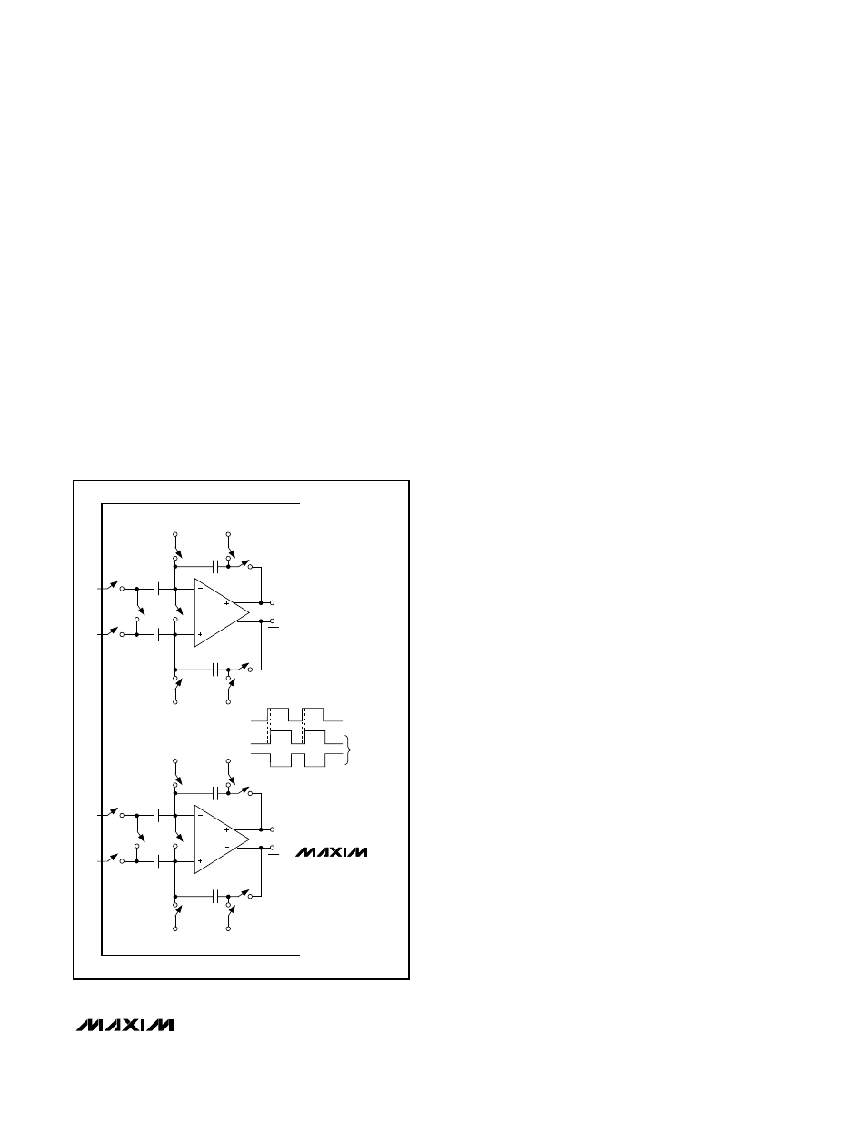
Input Track-and-Hold (T/H) Circuits
Figure 2 displays a simplified functional diagram of the
input track-and-hold (T/H) circuits in both track-and-
hold mode. In track mode, switches S1, S2a, S2b, S4a,
S4b, S5a, and S5b are closed. The fully differential cir-
cuits sample the input signals onto the two capacitors
(C2a and C2b) through switches S4a and S4b. S2a and
S2b set the common mode for the amplifier input, and
open simultaneously with S1, sampling the input wave-
form. Switches S4a and S4b are then opened before
switches S3a and S3b connect capacitors C1a and
C1b to the output of the amplifier and switch S4c is
closed. The resulting differential voltages are held on
capacitors C2a and C2b. The amplifiers are used to
charge capacitors C1a and C1b to the same values
originally held on C2a and C2b. These values are then
presented to the first stage quantizers and isolate the
pipelines from the fast-changing inputs. The wide input
bandwidth T/H amplifiers allow the MAX1183 to track
and sample/hold analog inputs of high frequencies (>
Nyquist). Both ADC inputs (INA+, INB+, INA- and INB-)
can be driven either differentially or single ended.
Match the impedance of INA+ and INA-, as well as
INB+ and INB- and set the common-mode voltage to
midsupply (V
DD
/2) for optimum performance.
Analog Inputs and Reference
Configurations
The full-scale range of the MAX1183 is determined by
the internally generated voltage difference between
REFP (V
DD
/2 + V
REFIN
/4) and REFN (V
DD
/2 -
V
REFIN
/4). The full-scale range for both on-chip ADCs is
adjustable through the REFIN pin, which is provided for
this purpose. REFOUT, REFP, COM (V
DD
/2), and REFN
are internally buffered low-impedance outputs. The
MAX1183 provides three modes of reference operation:
• Internal reference mode
• Buffered external reference mode
• Unbuffered external reference mode
In internal reference mode, connect the internal refer-
ence output REFOUT to REFIN through a resistor (e.g.,
10k
Ω) or resistor divider, if an application requires a
reduced full-scale range. For stability and noise filtering
purposes, bypass REFIN with a >10nF capacitor to
GND. In internal reference mode, REFOUT, COM, REFP,
and REFN become low-impedance outputs.
In buffered external reference mode, adjust the refer-
ence voltage levels externally by applying a stable and
accurate voltage at REFIN. In this mode, COM, REFP,
and REFN become outputs. REFOUT may be left open
or connected to REFIN through a >10k
Ω resistor.
In unbuffered external reference mode, connect REFIN
to GND. This deactivates the on-chip reference buffers
for REFP, COM, and REFN. With their buffers shut
down, these nodes become high impedance and may
be driven through separate, external reference
sources.
Clock Input (CLK)
The MAX1183’s CLK input accepts CMOS-compatible
clock signals. Since the interstage conversion of the
device depends on the repeatability of the rising and
falling edges of the external clock, use a clock with low
jitter and fast rise and fall times (<2ns). In particular,
sampling occurs on the rising edge of the clock signal,
requiring this edge to provide lowest possible jitter. Any
significant aperture jitter would limit the SNR perfor-
mance of the on-chip ADCs as follows:
MAX1183
Dual 10-Bit, 40Msps, +3V, Low-Power ADC with
Internal Reference and Parallel Outputs
______________________________________________________________________________________
11
S3b
S3a
COM
S5b
S5a
INB+
INB-
S1
OUT
OUT
C2a
C2b
S4c
S4a
S4b
C1b
C1a
INTERNAL
BIAS
INTERNAL
BIAS
COM
HOLD
HOLD
CLK
INTERNAL
NONOVERLAPPING
CLOCK SIGNALS
TRACK
TRACK
S2a
S2b
S3b
S3a
COM
S5b
S5a
INA+
INA-
S1
OUT
OUT
C2a
C2b
S4c
S4a
S4b
C1b
C1a
INTERNAL
BIAS
INTERNAL
BIAS
COM
S2a
S2b
MAX1183
Figure 2. MAX1183 T/H Amplifiers