Rainbow Electronics MAX533 User Manual
Page 7
MAX533
2.7V, Low-Power, 8-Bit Quad DAC
with Rail-to-Rail Output Buffers
_______________________________________________________________________________________
7
______________________________________________________________Pin Description
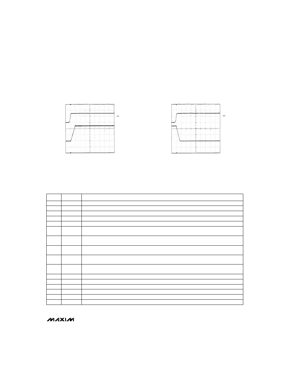
____________________________Typical Operating Characteristics (continued)
(V
DD
= +3V, T
A
= +25°C, unless otherwise noted.)
POSITIVE SETTLING TIME
MAX533-TOC15
5µs/div
CS
2V/div
OUTA
1V/div
V
DD
= 3.0V
V
REF
= 2.5V
DAC CODE = 01 TO FF hex
NO LOAD
NEGATIVE SETTLING TIME
MAX533-TOC16
5µs/div
CS
2V/div
OUTA
1V/div
V
DD
= 3.0V
V
REF
= 2.5V
DAC CODE = FF TO 00 hex
NO LOAD
PIN
DAC B Voltage Output
OUTB
1
FUNCTION
NAME
DAC A Voltage Output
OUTA
2
Software-Programmable Logic Output
UPO
4
Reference-Voltage Input
REF
3
Load DAC Input (active low). Driving this asynchronous input low (level sensitive) transfers the contents
of each input latch to its respective DAC latch.
LDAC
6
Serial Data Output. Sinks and sources current. Data at DOUT can be clocked out on the rising or falling
edge of SCLK (Table 1).
DOUT
8
Clear DAC Input (active low). Driving
CLR low asynchronously clears the input and DAC registers, and
sets all DAC outputs to zero.
CLR
7
Power-Down Enable. Must be high to enter software shutdown mode.
PDE
5
Serial Clock Input. Data is clocked in on the rising edge and clocked out on the falling (default) or rising
edge (A0 = A1 = 1, see Table 1).
SCLK
10
Digital Ground
DGND
12
Serial Data Input. Data is clocked in on the rising edge of SCLK.
DIN
11
Analog Ground
AGND
14
DAC C Voltage Output
OUTC
16
DAC D Voltage Output
OUTD
15
Power Supply, +2.7V to +3.6V
V
DD
13
Chip-Select Input (active low). Data is shifted in and out when
CS is low. Programming commands are
executed when
CS returns high.
CS
9