Max533, Table 2. unipolar code table – Rainbow Electronics MAX533 User Manual
Page 14
MAX533
Power Sequencing
The voltage applied to REF should not exceed V
DD
at
any time. If proper power sequencing is not possible,
connect an external Schottky diode between REF and
V
DD
to ensure compliance with the absolute maximum
ratings. Do not apply signals to the digital inputs before
the device is fully powered up.
Power-Supply Bypassing
and Ground Management
Connect AGND and DGND together at the IC. This
ground should then return to the highest-quality ground
available. Bypass V
DD
with a 0.1µF capacitor, located
as close to V
DD
and DGND as possible.
Careful PC board layout minimizes crosstalk among
DAC outputs and digital inputs. Figure 10 shows sug-
gested circuit board layout to minimize crosstalk.
Unipolar-Output,
Two-Quadrant Multiplication
In unipolar operation, the output voltages and the refer-
ence input are the same polarity. Figure 11 shows the
MAX533 unipolar configuration, and Table 2 shows the
unipolar code.
2.7V, Low-Power, 8-Bit Quad DAC
with Rail-to-Rail Output Buffers
14
______________________________________________________________________________________
Table 2. Unipolar Code Table
1
Note:
1LSB = (V
REF
) (2
-8
) = +V
REF
(
––––
)
256
1
+V
REF
(
––––
)
256
0 0 0 1
0 0 0 0
0V
0 0 0 0
0 0 0 0
127
+V
REF
(
––––
)
256
1 1 1 1
0 1 1 1
128 V
REF
+V
REF
(
––––
)
= + –
–––
256 2
0 0 0 0
1 0 0 0
129
+V
REF
(
––––
)
256
0 0 0 1
1 0 0 0
255
+V
REF
(
––––
)
256
1 1 1 1
1 1 1 1
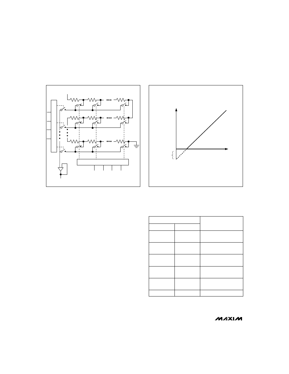
ANALOG
OUTPUT
LSB
MSB
DAC CONTENTS
DAC CODE
0V
NEGATIVE
OFFSET
OUTPUT
VOLTAGE
Figure 9. Effect of Negative Offset (Single Supply)
R1
R0
REF
D7
D5
D6
D4
R15
R16
R255
LSB DECODER
D2
D3
DAC A
D1
D0
MSB DECODER
Figure 8. DAC Simplified Circuit Diagram