Applications information – Rainbow Electronics MAX533 User Manual
Page 13
MAX533
2.7V, Low-Power, 8-Bit Quad DAC
with Rail-to-Rail Output Buffers
______________________________________________________________________________________
13
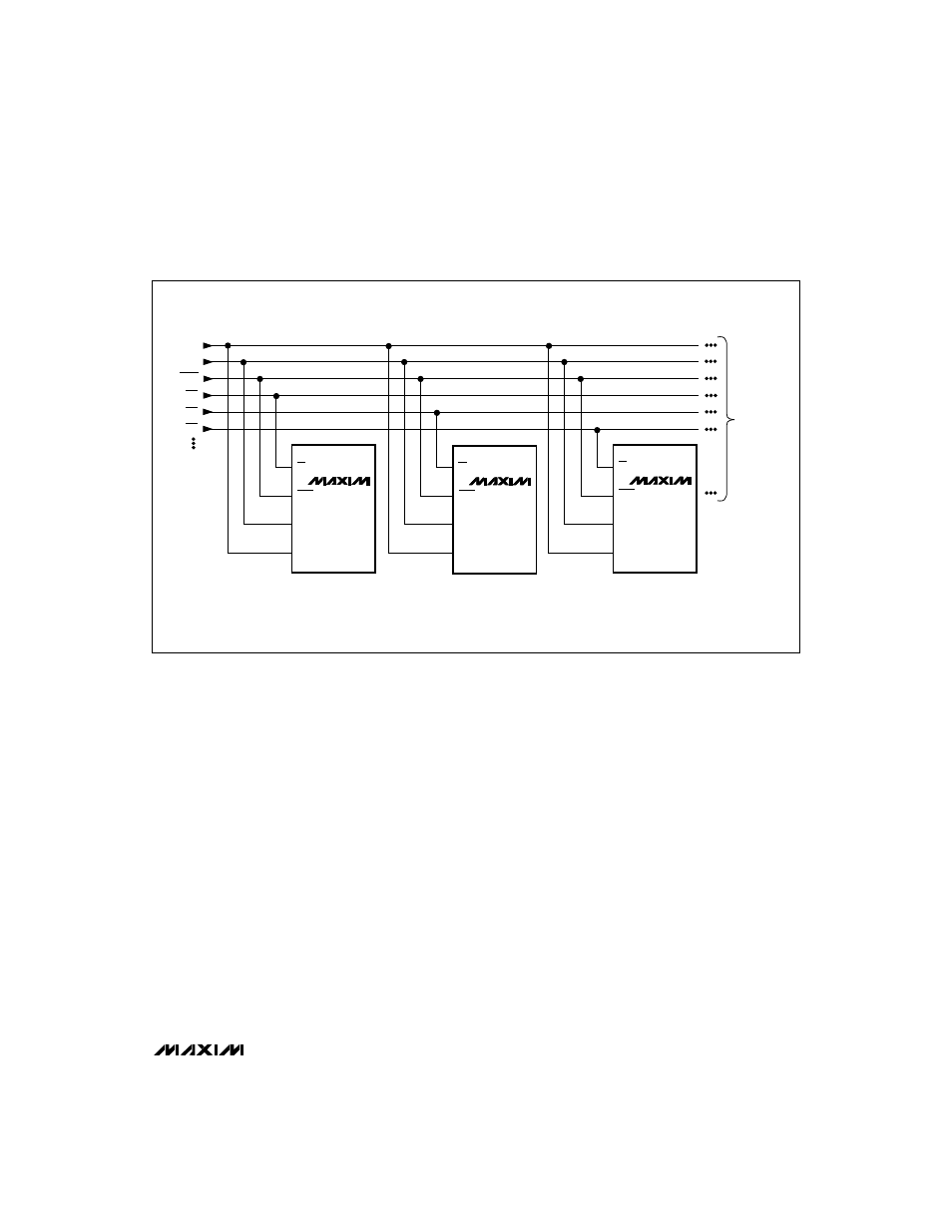
CS
LDAC
SCLK
DIN
MAX533
CS
LDAC
SCLK
DIN
MAX533
CS
LDAC
SCLK
DIN
MAX533
TO OTHER
SERIAL
DEVICES
DIN
SCLK
LDAC
CS1
CS2
CS3
Figure 7. Multiple MAX533s sharing one DIN line. Simultaneously update by strobing
LDAC, or specifically update by enabling an
individual
CS.
Output Buffer Amplifiers
All MAX533 voltage outputs are internally buffered by
precision unity-gain followers that slew at about
0.6V/µs. The outputs can swing from GND to V
DD
. With
a 0V to +2.5V (or +2.5V to 0V) output transition, the
amplifier outputs will typically settle to 1/2LSB in 6µs
when loaded with 10k
Ω
in parallel with 100pF.
The buffer amplifiers are stable with any combination of
resistive (
≥
10k
Ω
) or capacitive loads.
__________Applications Information
DAC Linearity and Voltage Offset
The output buffer can have a negative input offset volt-
age that would normally drive the output negative, but
since there is no negative supply the output stays at 0V
(Figure 9). When linearity is determined using the end-
point method, it is measured between zero code (all
inputs 0) and full-scale code (all inputs 1) after offset
and gain error are calibrated out. However, in single-
supply operation the next code after zero may not
change the output (Figure 9), so the lowest code that
produces a positive output is the lower endpoint.