Rainbow Electronics MAX533 User Manual
Page 10
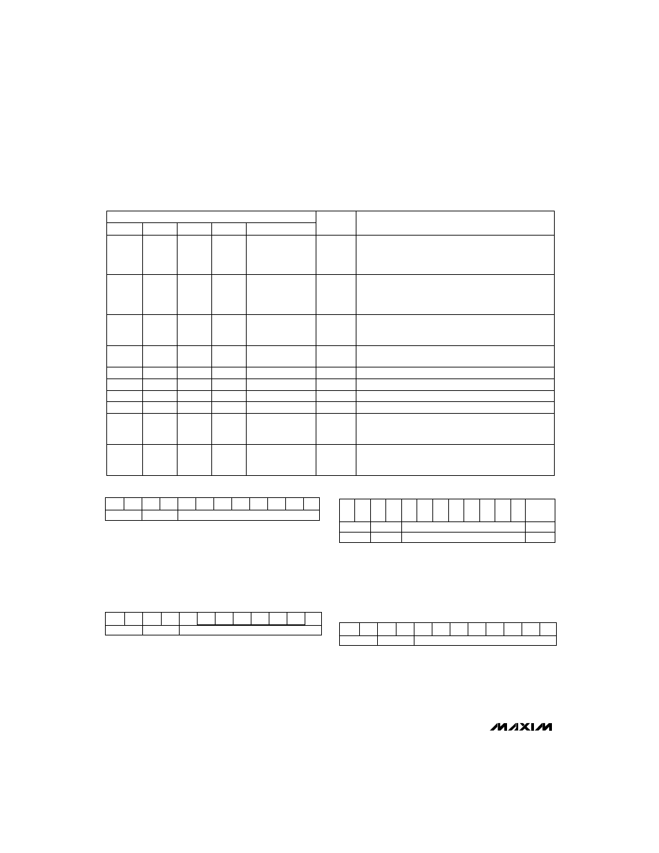
Load All DACs with Shift-Register Data
All four DAC registers are updated with shift-register
data. This command allows all DACs to be set to any
analog value within the reference range. This command
can be used to substitute
CLR if code 00 hex is pro-
grammed, which clears all DACs.
Software Shutdown
Shuts down all output buffer amplifiers, reducing sup-
ply current to 10µA max.
User-Programmable Output (UPO)
User-programmable logic output for controlling another
device across an isolated interface. Example devices
are gain control of an amplifier, a 4mA to 20mA amplifi-
er, and a polarity output for a motor speed control.
No Operation (NOP)
The NOP command (no operation) allows data to be
shifted through the MAX533 shift register without affect-
ing the input or DAC registers. This is useful in daisy
chaining (also see the
Daisy Chaining Devices section).
MAX533
2.7V, Low-Power, 8-Bit Quad DAC
with Rail-to-Rail Output Buffers
10
______________________________________________________________________________________
Set DOUT phase—SCLK rising (mode 1). DOUT
clocked out on rising edge of SCLK. All DACs updated
from their respective input registers.
Software shutdown (provided PDE is high)
Load all DACs with shift-register data. Also bring the
part out of shutdown mode.
12-BIT SERIAL WORD
0
0
1
1
0
0
1
1
C0
0
0
0
0
1
1
1
1
1
1
1
1
C1
1
0
0
0
1
1
1
1
0
0
0
0
A0
1
1
0
1
0
1
0
1
0
1
0
1
FUNCTION
LDAC
D7 . . . . . . . . D0
A1
X
X X X X X X X X
1
X
X X X X X X X X
1
X
8-bit DAC data
1
Software
LDAC commands. Update all DACs from
their respective input registers. Also bring the part out
of shutdown mode.
1
X X X X X X X X
0
Load input register A; all DAC outputs updated
Load input register B; all DAC outputs updated
Load input register C; all DAC outputs updated
Load input register D; all DAC outputs updated.
1
1
1
1
8-bit DAC data
8-bit DAC data
8-bit DAC data
8-bit DAC data
Load input register A; all DAC outputs unchanged.
Load input register B; all DAC outputs unchanged.
Load input register C; all DAC outputs unchanged.
Load input register D; all DAC outputs unchanged.
1
1
1
1
8-bit DAC data
8-bit DAC data
8-bit DAC data
8-bit DAC data
UPO goes low.
0
1
0
X
X X X X X X X X
0
UPO goes high.
0
No operation (NOP); shift data in shift registers.
1
0
1
0
X
X X X X X X X X
0
0
X
X X X X X X X X
0
Set DOUT phase—SCLK falling (mode 0). DOUT
clocked out on falling edge of SCLK. All DACs up-
dated from their respective registers (default).
0
1
0
X
X X X X X X X X
1
(
LDAC = X)
(
LDAC = X, PDE = H)
(
LDAC = X)
(
LDAC = X)
A1
A0
C1
C0
D7
D6
D5
D4
D3
D2
D1
D0
1 0
0 0
8-Bit Data
A1
A0
C1
C0
D7
D6
D5
D4
D3
D2
D1
D0
1 1
0 0
x
x
x
x
x
x
x
x
UPO
Output
A1 A0 C1 C0 D7 D6 D5 D4 D3 D2 D1 D0
0 0
1 0
x
x
x
x
x
x
x
x
Low
0 1
1 0
x
x
x
x
x
x
x
x
High
x
x
x
x
x
x
x
x
0 0
0 0
D0
D1
D2
D3
D4
D5
D6
D7
C0
C1
A0
A1