Timing characteristics (continued) – Rainbow Electronics MAX533 User Manual
Page 4
MAX533
2.7V, Low-Power, 8-Bit Quad DAC
with Rail-to-Rail Output Buffers
4
_______________________________________________________________________________________
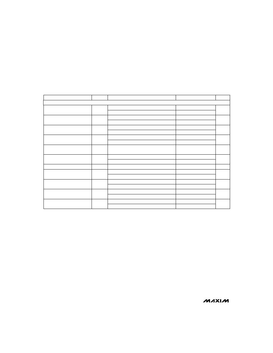
TIMING CHARACTERISTICS (continued)
(V
DD
= +2.7V to +3.6V, V
REF
= 2.5V, AGND = DGND = 0V, C
DOUT
= 100pF, T
A
= T
MIN
to T
MAX
, unless otherwise noted.
Typical values are at V
DD
= +3V and T
A
= +25°C.)
Note 1:
INL and DNL are measured with R
L
referenced to ground. Nonlinearity is measured from the first code that is greater than
or equal to the maximum offset specification to code FF hex (full scale). See
DAC Linearity and Voltage Offset
section.
Note 2:
V
REF
= 2.5Vp-p, 10kHz. Channel-to-channel isolation is measured by setting one DAC’s code to FF hex and setting all
other DAC’s codes to 00 hex.
Note 3:
V
REF
= 2.5Vp-p, 10kHz. DAC code = 00 hex.
Note 4:
Guaranteed by design, not production tested.
Note 5:
Output settling time is measured from the 50% point of the rising edge of
CS to 1/2LSB of V
OUT
’s final value.
Note 6:
Digital crosstalk is defined as the glitch energy at any DAC output in response to a full-scale step change on any other
DAC.
Note 7:
If
LDAC is activated prior to CS’s rising edge, it must stay low for t
LDAC
or longer after
CS goes high.
Note 8:
When DOUT is not used. If DOUT is used, f
CLK
max is 4MHz, due to the SCLK to DOUT propagation delay.
Note 9:
Serial data clocked out at SCLK’s rising edge (measured from 50% of the clock edge to 20% or 80% of V
DD
).
Note 10:
Serial data clocked out at SCLK’s falling edge (measured from 50% of the clock edge to 20% or 80% of V
DD
).
CS Rise to SCLK Rise Setup
Time
t
CS1
50
ns
SCLK Rise to
CS Fall Delay
t
CS0
50
ns
MAX533M
MAX533M
40
40
MAX533C/E
MAX533C/E
SCLK Fall to DOUT Valid
Propagation Delay (Note 10)
t
DO2
250
ns
MAX533M
210
MAX533C/E
SCLK Rise to DOUT Valid
Propagation Delay (Note 9)
t
DO1
230
ns
MAX533M
200
MAX533C/E
40
CS Fall to SCLK Rise Setup
Time
t
CSS
50
40
ns
SCLK Pulse Width Low
t
CL
50
ns
MAX533C/E
MAX533M
MAX533C/E
MAX533M
40
SCLK Pulse Width High
t
CH
50
ns
MAX533C/E
MAX533M
PARAMETER
SYMBOL
MIN
TYP
MAX
UNITS
SERIAL-INTERFACE TIMING
10
SCLK Clock Frequency (Note 8)
f
CLK
8.3
MHz
SCLK Rise to
CS Rise Hold Time
t
CSH
0
ns
40
DIN to SCLK Rise to Setup Time
t
DS
50
DIN to SCLK Rise to Hold Time
t
DH
0
ns
CONDITIONS
MAX533C/E
MAX533M
MAX533C/E
MAX533M