Chip topographies – Rainbow Electronics MAX913 User Manual
Page 8
Maxim cannot assume responsibility for use of any circuitry other than circuitry entirely embodied in a Maxim product. No circuit patent licenses are
implied. Maxim reserves the right to change the circuitry and specifications without notice at any time.
8
___________________Maxim Integrated Products, 120 San Gabriel Drive, Sunnyvale, CA 94086 (408) 737-7600
© 1994 Maxim Integrated Products
Printed USA
is a registered trademark of Maxim Integrated Products.
MAX912/MAX913
Single/Dual, Ultra-Fast, Low-Power,
Precision TTL Comparators
HYSTERESIS
BAND*
IN+
IN-
Q
* WHEN HYSTERESIS IS ADDED, A COMPARATOR CANNOT RESOLVE ANY INPUT SIGNAL WITHIN THE HYSTERESIS BAND.
WITH HYSTERESIS
IDEAL (WITHOUT HYSTERESIS)
.
.
.
.
.
.
.
.
.
.
.
.
..
Figure 2. Effect of Hysteresis on Input Resolution
supply pins, keeping leads short to minimize lead
inductance. For particularly noisy applications, use fer-
rite beads on the power-supply lines.
Board Layout
As with all high-speed components, careful attention to
layout is essential for best performance.
1) Use a printed circuit board with an unbroken
ground plane.
2) Pay close attention to the bandwidth of bypass
components and keep leads short.
3) Avoid sockets; solder the comparator and other
components directly to the board to minimize
unwanted parasitic inductance and capacitance.
Input Slew Rate
The MAX912/MAX913 design eliminates the input slew-
rate requirement imposed on many standard compara-
tors. As long as LE is high after the maximum propaga-
tion delay and the input is greater than the compara-
tor’s total DC error, the output will be valid without oscil-
lations.
Maximum Clock (LE) and Signal Rate
The maximum clock and signal rate is 70MHz, based
on the comparator’s rise and fall time with a 5mV over-
drive at +25°C (Figure 1). With a 20mV overdrive, the
maximum propagation delay is 12ns and the clock and
signal rate is 85MHz.
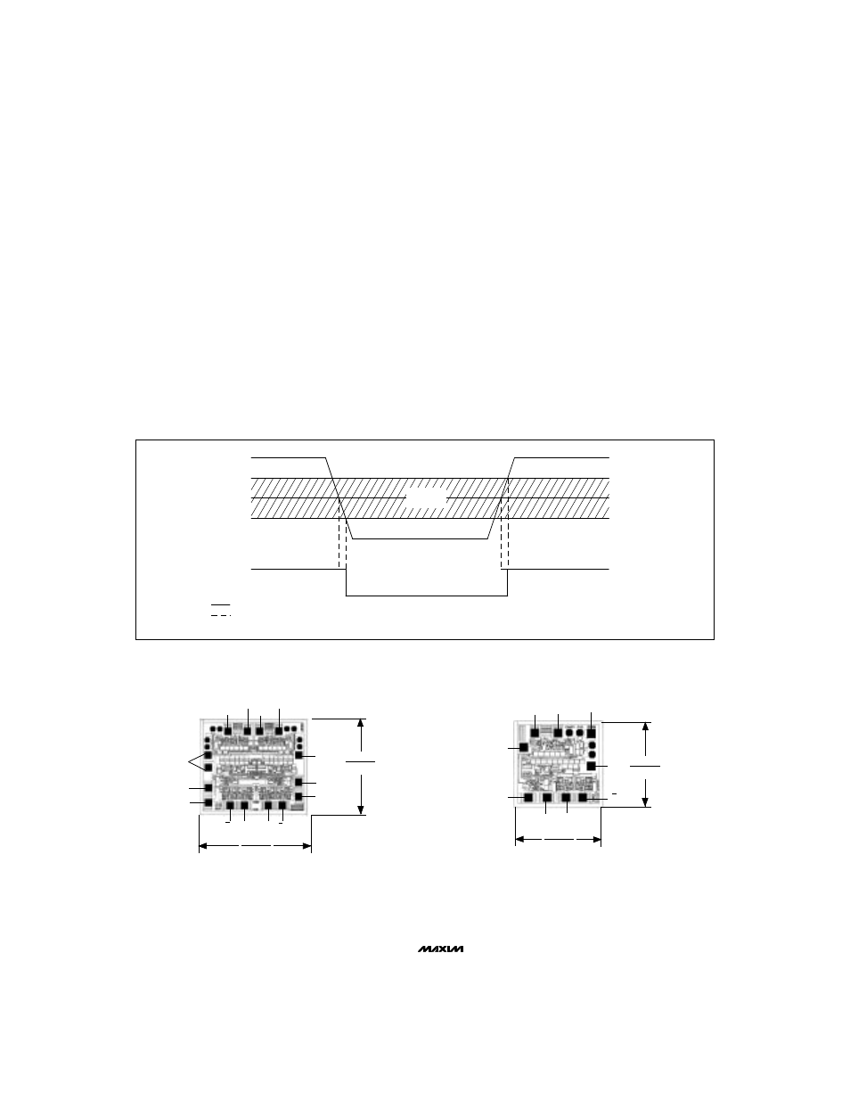
__________________________________________________________Chip Topographies
V-
LEA
LEB
GND
INB-
QB
0.071"
(1.80mm)
0.080"
(2.03mm)
INB+
INA+
INA-
GND
QB
QA QA
V+
V+
V-
LE
IN-
0.056"
(1.42mm)
0.058"
(1.47mm)
IN+
V+
Q
GND
Q
MAX913
MAX912
TRANSISTOR COUNT: 100;
SUBSTRATE CONNECTED TO V-.
TRANSISTOR COUNT: 197;
SUBSTRATE CONNECTED TO V-.